Photomask defect correction method employing a combined device of a focused electron beam device and an atomic force microscope

Active Publication Date: 2005-12-29
HITACHI HIGH TECH SCI CORP
View PDF5 Cites 18 Cited by
  • Summary
  • Abstract
  • Description
  • Claims
  • Application Information

AI Technical Summary

Benefits of technology

[0021] By using a device where the focused electron beam and the AFM scratch unit are in a vacuum, it is possible to shorten the time of taking out and inserting the mask and performing mas

Problems solved by technology

It is therefore not possible to know the positions and shapes of defects even when an optical microscope is at maximum magnification because the defects are too small.
Image acquisition therefore has to be carried out using an AFM image, which is time-consuming.
It is also difficult to search for defects with a field of vision of 40 μm even with an AFM image.
Finding the positions of the defects is therefore more time-consuming than the processing.
Because of this, it is therefore necessary to carry out mask alignment so as to re-link the defect scanning device and defect coordinates so as to obtain an image and then perform a time-consuming search for defects using an AFM image, which is still more time-consuming.
In addition to opaque defects that are surplus to a pattern in a photomask, there also exist clear defects that are pattern deficiencies, and in theory, it is not possible for the AFG scratch processing device to correct clear defects.
However, various problems occur such as thin films of 0.1 μm or less not becoming attached, sagging occurring in the shapes of the films so that transmittance is lowered by a hollow component, and charging up occurring in order to correct a ph

Method used


Image

  • Photomask defect correction method employing a combined device of a focused electron beam device and an atomic force microscope
  • Photomask defect correction method employing a combined device of a focused electron beam device and an atomic force microscope
  • Photomask defect correction method employing a combined device of a focused electron beam device and an atomic force microscope

Examples


Embodiment Construction

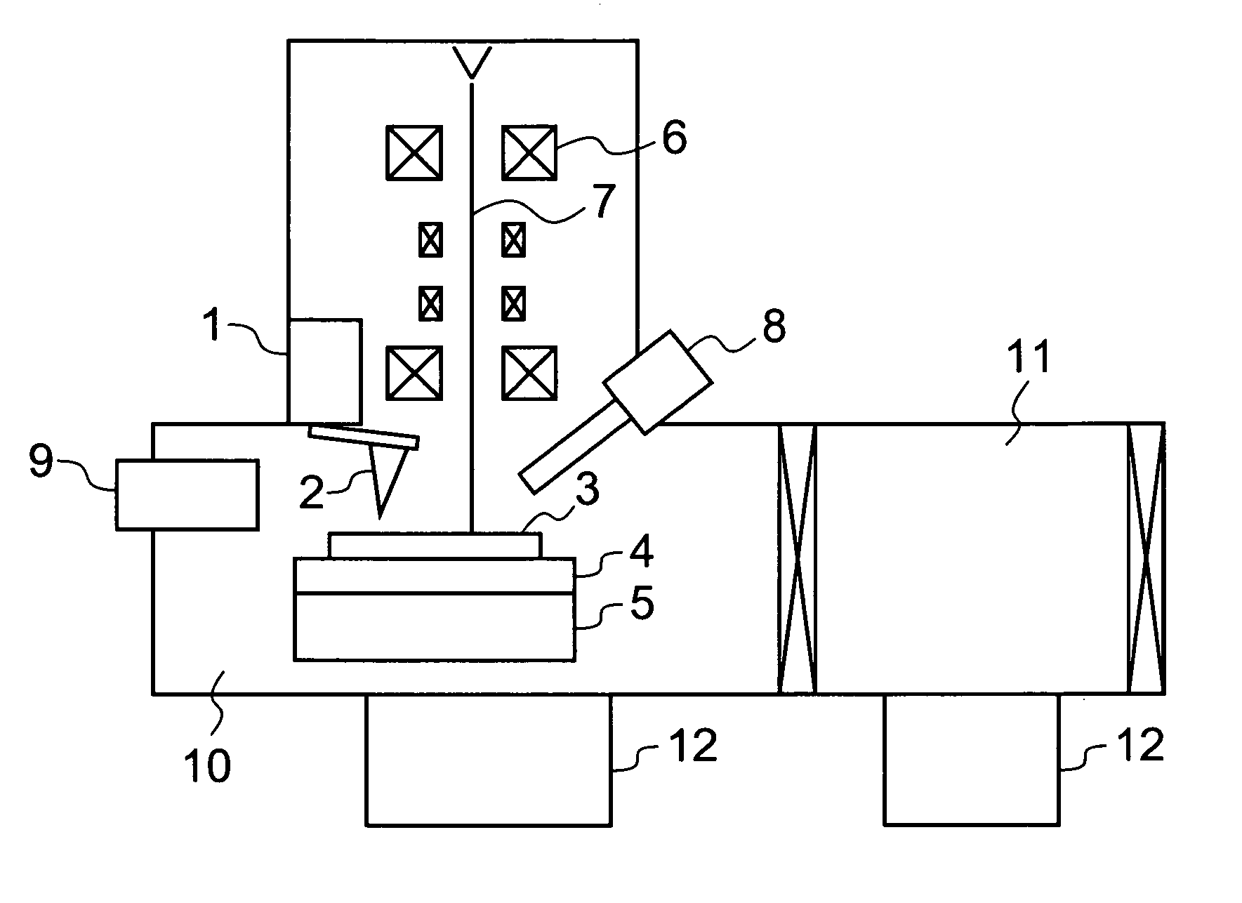
[0026] The following is a description of an embodiment of the present invention. FIG. 1 shows a combined device of a focused electron beam and AFM used in the present invention. A photomask 3 for which a defect has been found using a defect scanning device is introduced into a pre-chamber 11 of a device combining an electro-optical system 6 and an atomic force microscope (AFM) head 1 within a container having a vacuum evacuation system 12, and preliminary evacuation is carried out. When a vacuum is created in the preliminary chamber, the photomask 3 is moved into a work chamber 10. An alignment mark of the mask is then observed at a high-magnification by detecting secondary electrons generated from the sample owing to irradiation of the focused electron beam 7 with the secondary electron detector 9 and mask alignment (alignment of the defect scanning device and coordinate starting points) is carried out. Alignment mark alignment can also be carried out at a higher precision than in ...


PUM


Abstract

In order to make it possible to improve throughput of AFM scratch processing, enable correction of small defects in clear defect correction with a high degree of precision, and enable correction in a shorter period of time in the event of overcutting by AFM scratch processing, throughput of AFM scratch processing is increased by maximizing high-resolution of the electron beam device and minimizing the time taken in observations using a device incorporating both an electro-optical system and an AFM head in a vacuum, correcting small clear defects with high precision by eliminating portions left over from AFM scratch processing after applying a clear defect correction film using an electron beam while providing light-blocking film raw material, and correction in a short time is made possible by eliminating portions remaining using AFM scratch processing after applying a clear defect correction film using an electron beam while providing light-blocking film raw material also in cases of overcutting in AFM scratch processing.

Description

BACKGROUND OF THE INVENTION [0001] 1. Field of the Invention [0002] The present invention relates to a photomask defect correction method employing a combined device of a focused electron beam device and an atomic force microscope. [0003] 2. Description of the Related Art [0004] As fine detailing of patterns becomes smaller, photomask defects of an original plate of a pattern transfer for a wafer to be corrected also become small, and high-precision correction can also be obtained. Further, optical proximity correction (OPC) patterns that are even smaller patterns for correcting optical proximity results so as to increase resolving power have also been introduced which means that it is also necessary to correct defects of OPC patterns that are smaller than these patterns. In addition to defect correction devices employing lasers and focused electron beams of the related art, it is also possible to carry out scratch processing of physically eliminating opaque defects using a diamond ...

Claims


Application Information

Patent Timeline
IPC IPC(8): G01N13/16G01N23/00G03F1/72G21K7/00H01L21/027
CPCB82Y35/00G01N23/00G01Q30/02Y10S977/856G01Q80/00G03F1/72G03F1/74G01Q60/24
Inventor TAKAOKA, OSAMUHAGIWARA, RYOJI
Owner HITACHI HIGH TECH SCI CORP
Why Eureka
Try Eureka