
Gapless microlens array and method of fabrication

a technology of microlens and arrays, applied in the field of gapless microlens arrays and fabrication methods, can solve the problems of increasing difficulty in providing a microlens capable of focusing incident light rays onto the photosensitive regions of the pixel cell, spherical microlenses, and increased difficulty in constructing microlenses

Active Publication Date: 2005-12-22
APTINA IMAGING CORP
View PDF20 Cites 42 Cited by
  • Summary
  • Abstract
  • Description
  • Claims
  • Application Information

AI Technical Summary

Benefits of technology

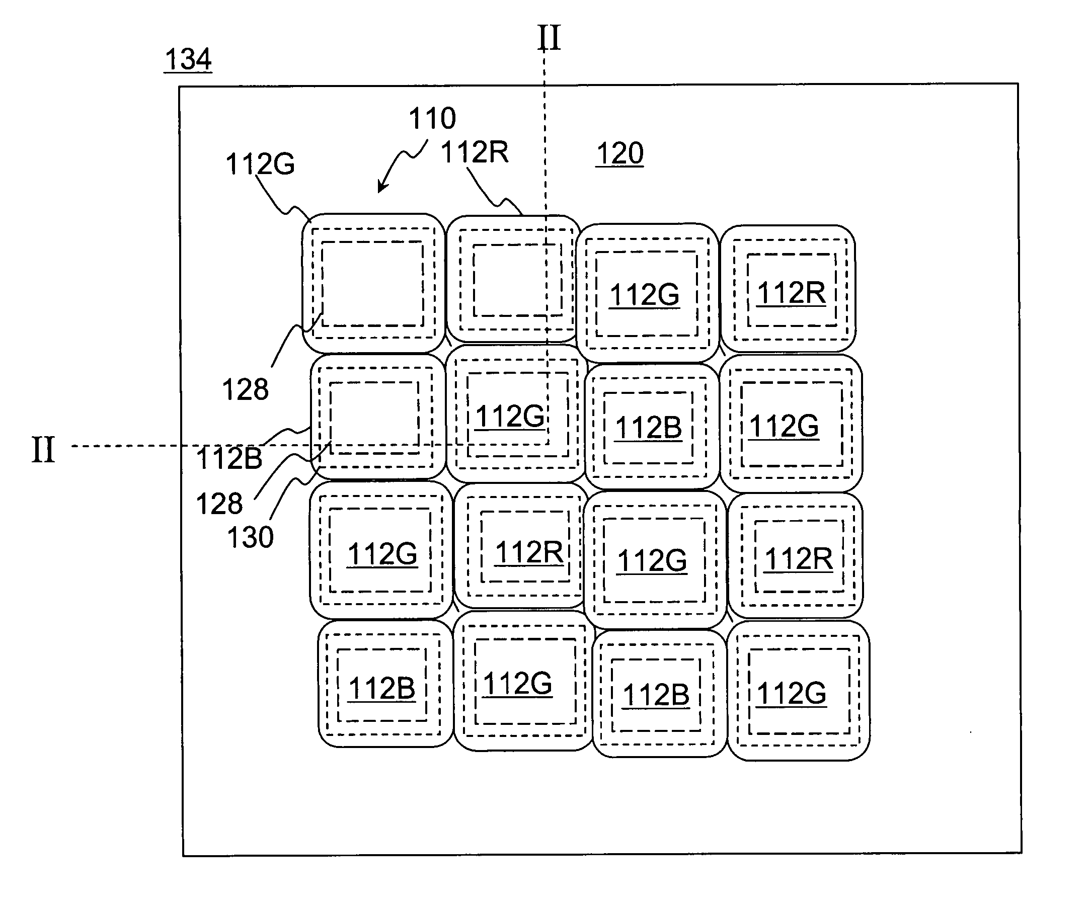
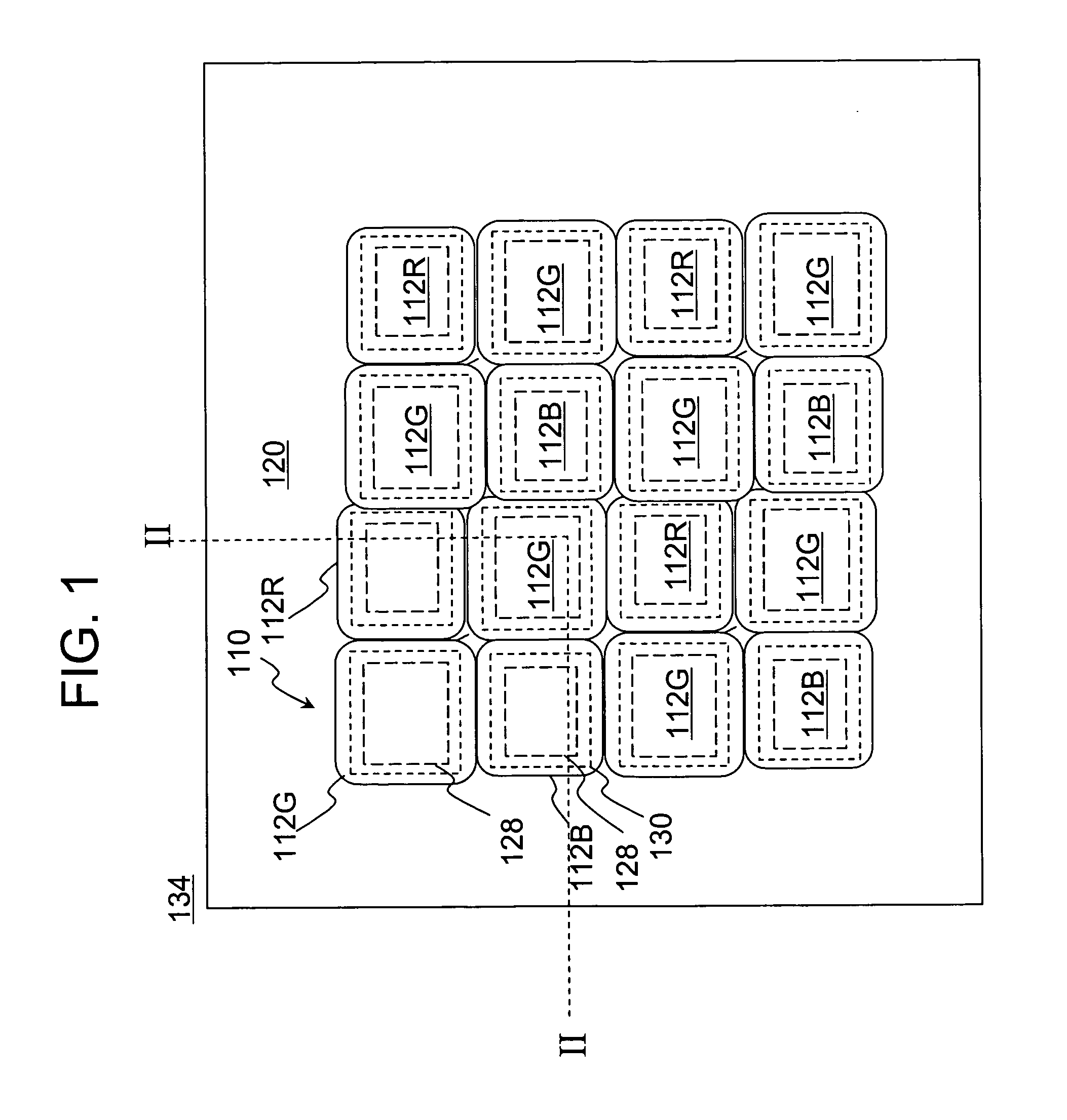
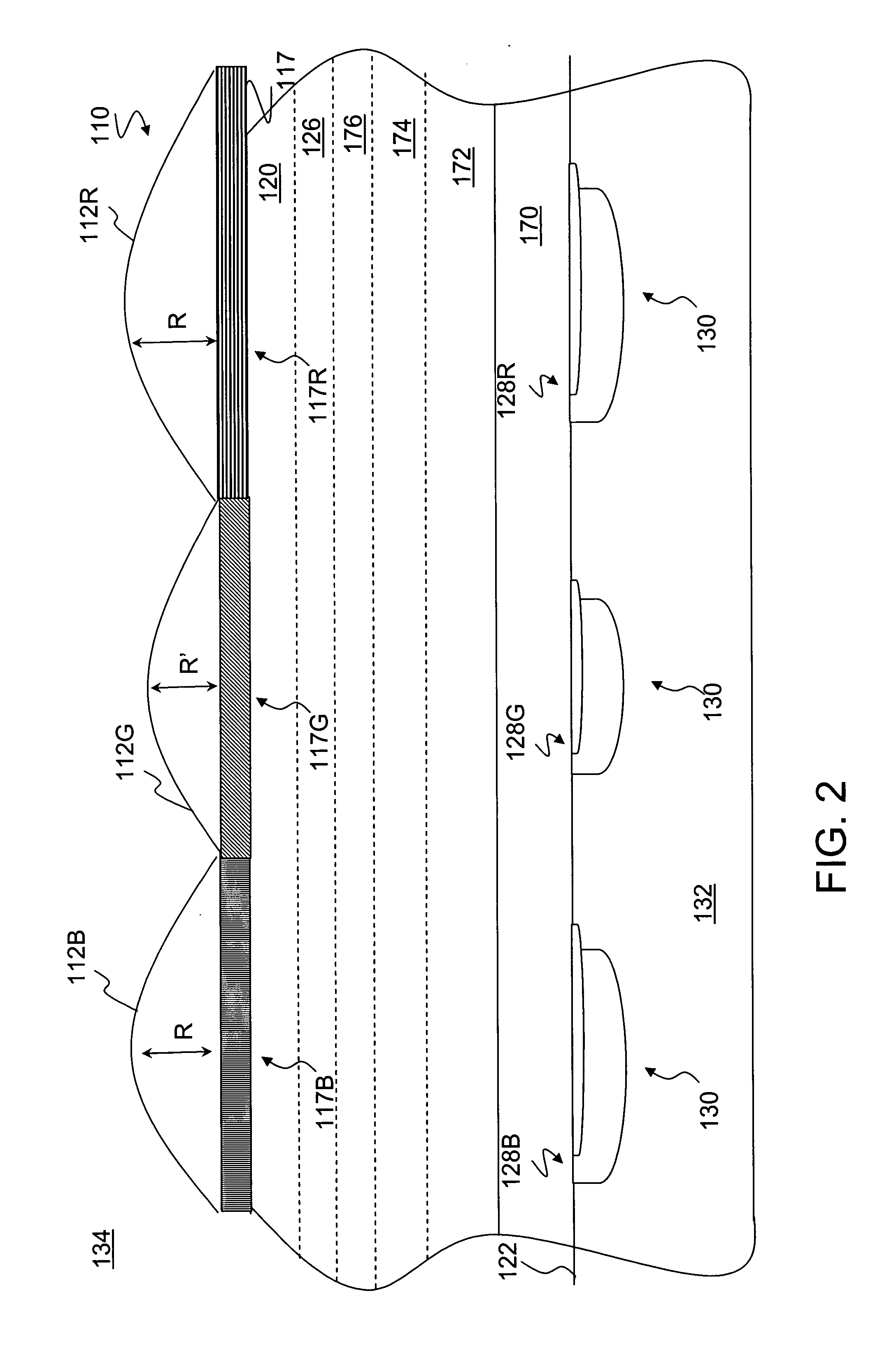
The invention is about a microlens array with no empty space between the lenses and a method for making it. The lenses also have a shifted focal point, which directs photon radiation towards asymmetrically formed photosensors. This results in improved image quality and reduced blurring.

Problems solved by technology

As the size of imager arrays and photosensitive regions of pixels continue to decrease, it becomes increasingly difficult to provide a microlens capable of focusing incident light rays onto the photosensitive regions of the pixel cell.
This problem is due in part to the increased difficulty in constructing a microlens that has the optimal focal characteristics for the increasingly smaller imager device.
Spherical microlenses, however, suffer from gapping problems which are undesirable as described below.
A change in the energy distribution in the focal range leads to a loss in quantum efficiency of, and enhanced cross-talk between, pixels.
On the other hand, if the gapping is too wide during fabrication, the gaps allow unfocused photons through the empty spaces in the microlens array, leading to lower quantum efficiency and increased cross-talk between respective photosensors of adjacent pixel cells.
Due to the use of pixel cell arrays having asymmetrical architecture, the formation of microlenses through conventional processes leads to bridging and / or gapping, which results in lower quantum efficiency, as discussed above.

Method used


Image

  • Gapless microlens array and method of fabrication
  • Gapless microlens array and method of fabrication
  • Gapless microlens array and method of fabrication

Examples


Embodiment Construction

[0020] In the following detailed description, reference is made to the accompanying drawings, which form a part hereof and show by way of illustration specific embodiments in which the invention may be practiced. These embodiments are described in sufficient detail to enable those skilled in the art to practice the invention, and it is to be understood that other embodiments may be utilized, and that structural, logical, and electrical changes may be made without departing from the spirit and scope of the present invention. The progression of processing steps described is exemplary of embodiments of the invention; however, the sequence of steps is not limited to that set forth herein and may be changed as is known in the art, with the exception of steps necessarily occurring in a certain order.

[0021] As used herein, the terms “semiconductor substrate” and “substrate” are to be understood to include any semiconductor-based structure. The semiconductor structure should be understood ...


PUM

PropertyMeasurementUnit
distanceaaaaaaaaaa
focal lengthaaaaaaaaaa
distanceaaaaaaaaaa

Abstract

A microlens array with reduced or no empty space between individual microlenses and a method for forming the same. The microlens array is formed by patterning a first set of microlens precursors in a checkerboard pattern on a substrate. The first set of microlens precursors is reflowed and cured into first microlenses impervious to subsequent reflows. Then, a second set of microlens precursors is patterned in spaces among the first microlenses, reflowed and cured into second microlenses. The reflows and cures can be conducted under different conditions, and the microlenses may be differently sized. The conditions of the reflows can be chosen to ensure that the focal lengths of microlenses are optimized for maximum sensor signal.

Description

CROSS REFERENCE TO RELATED APPLICATIONS [0001] This application is a continuation in-part of application Ser. No. 10 / 681,308, filed Oct. 9, 2003, and application Ser. No. 11 / 002,231, filed on Dec. 3, 2004, which are hereby incorporated by reference.FIELD OF THE INVENTION [0002] The invention relates generally to imaging devices and, more particularly to an array of microlenses over an asymmetrical photosensor array used to focus light on said photosensor array, and the method of making said array. BACKGROUND OF THE INVENTION [0003] Imaging devices, including charge coupled devices (CCD) and complementary metal oxide semiconductor (CMOS) sensors have commonly been used in photo-imaging applications. A CMOS imager circuit includes a focal plane array of pixel cells, each one of the cells including a photosensor, for example, a photo gate, photo conductor or a photo diode for accumulating photo-generated charge in the specified portion of the substrate. Each pixel cell has a charge sto...

Claims


Application Information

Patent Timeline
Patent Type & Authority Applications(United States)
IPC IPC(8): B29D11/00G02B3/00
CPCB29D11/00278B29D11/00365G02B3/0018H01L27/14627G02B3/005G02B3/0056H01L27/14621G02B3/0043H01L27/14605H01L27/14685
Inventor BOETTIGER, ULRICH C.LI, JIN
Owner APTINA IMAGING CORP
Learn More