
Method for testing contact open in semiconductor device

a technology for semiconductor devices and contact open, which is applied in the testing/measurement of individual semiconductor devices, semiconductor/solid-state devices, instruments, etc., can solve the problems of increasing process inefficiency, generating contact defects, and reducing the efficiency of process yields, so as to achieve effective testing of contact open defects and secure mass productivity

Inactive Publication Date: 2005-12-08
SK HYNIX INC
View PDF0 Cites 3 Cited by
  • Summary
  • Abstract
  • Description
  • Claims
  • Application Information

AI Technical Summary

Benefits of technology

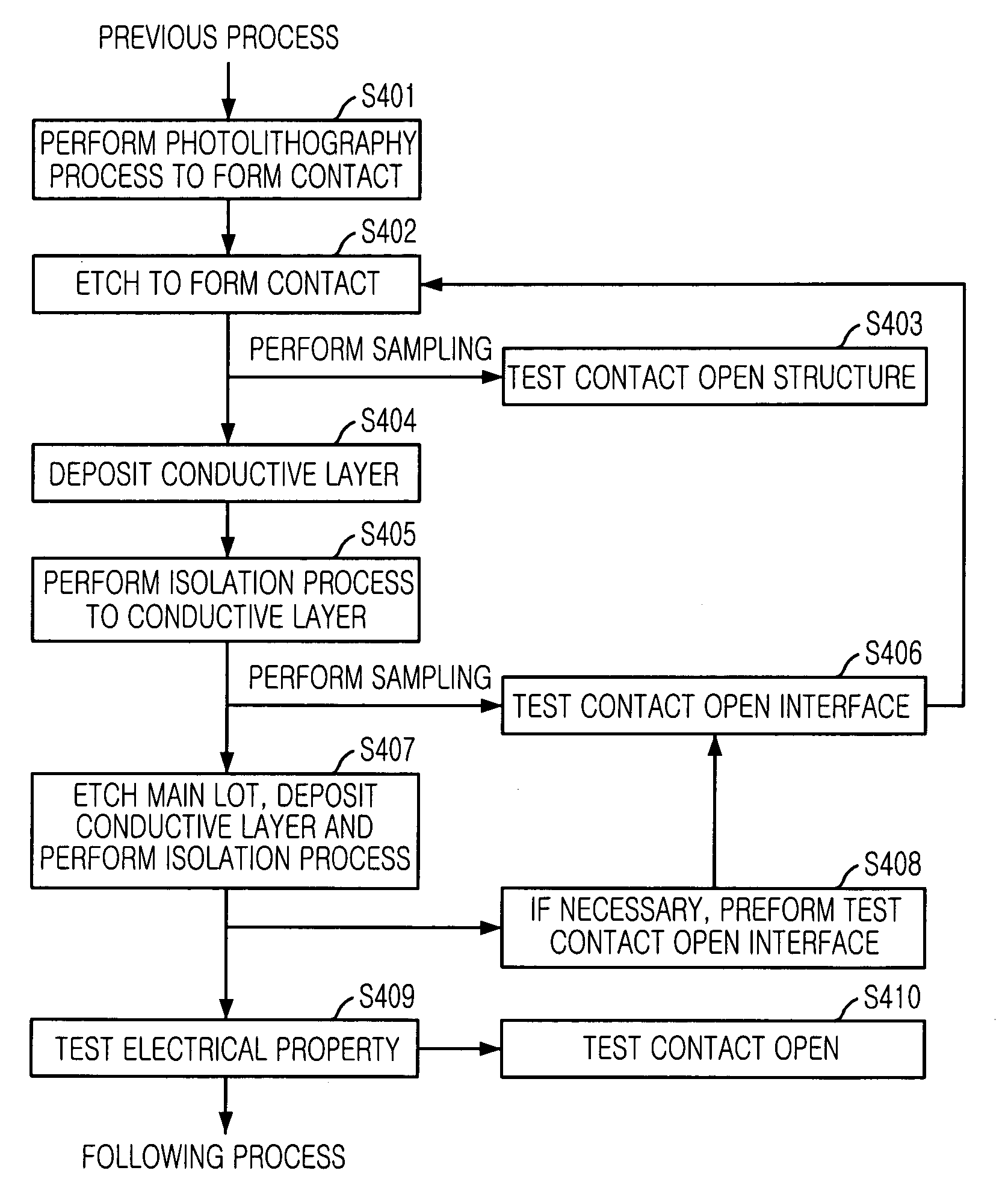
The present invention provides a method for testing a contact open, which can effectively detect defects in the manufacturing process of integrated circuits. This method involves forming a contact, sampling the wafer, etching the contact hole, depositing a conductive layer, isolating the conductive layer, testing the contact open interface, and etching the contact of a main lot based on the test result. This method ensures mass productivity and improves the reliability of the integrated circuits.

Problems solved by technology

A contact defect is resulted from various reasons.
For instance, when the photoresist in the contact hole is not completely removed during the photolithography process or the insulation layer in the contact hole is not completely removed during the etching process, the contact defect is generated.
Accordingly, an inefficiency is caused in yields of products and a process due to a long testing period.
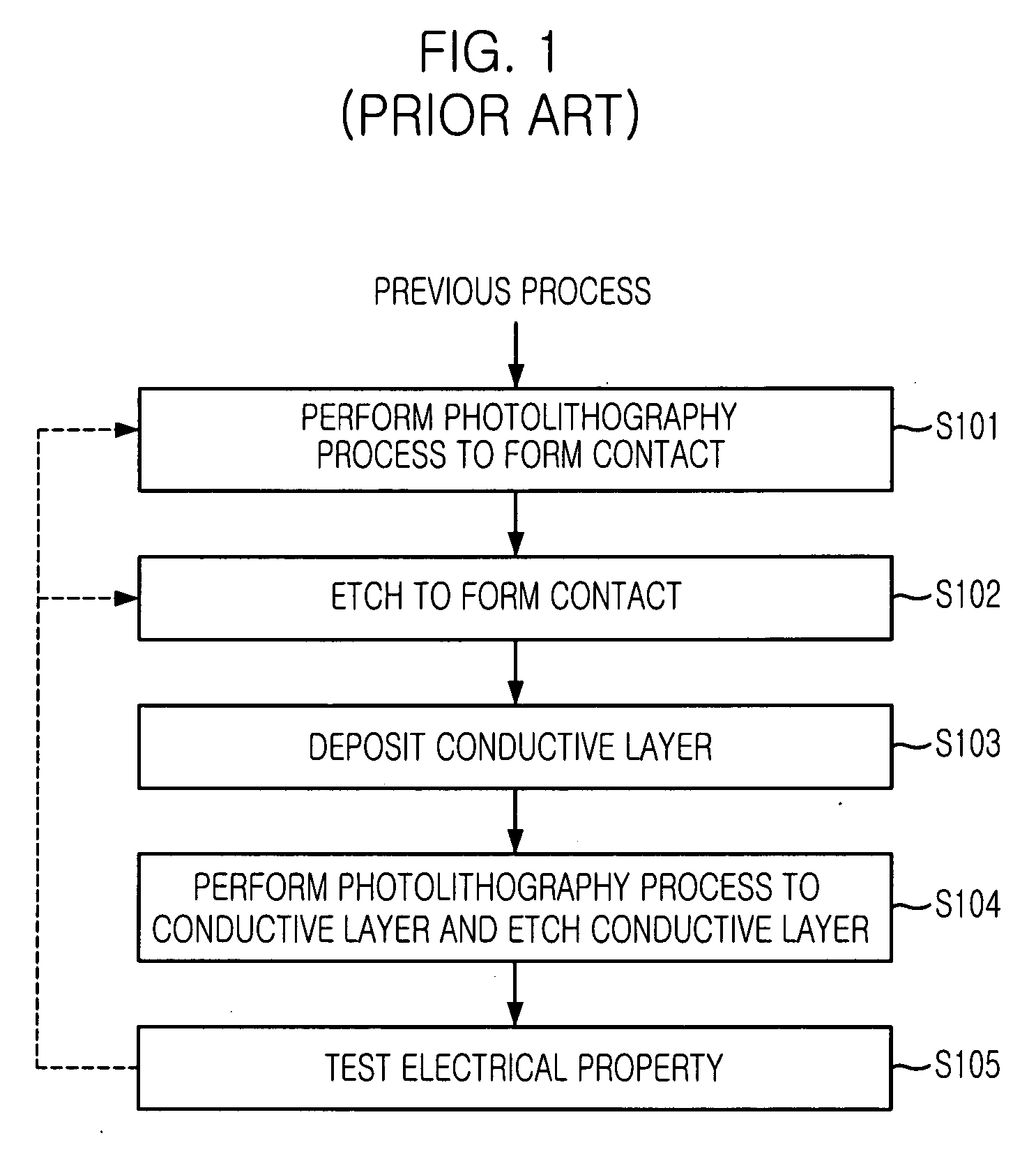
Therefore, the first preferred embodiment in accordance with the conventional method makes it difficult to predict the yields of the products in advance, thereby generating a problem of greatly increasing the inefficiency in the process.
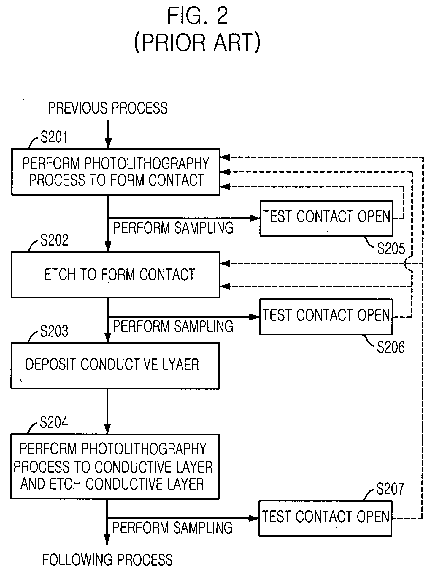
However, in accordance with the second preferred embodiment, it is required to sample and test at every each step and thus, it is difficult to apply the second preferred embodiment to an actual process.
Also, the second preferred embodiment provides a disadvantage that cannot accurately check the contact defect resulted from a defect between interfaces of the conductive layer and the substrate.

Method used


Image

  • Method for testing contact open in semiconductor device
  • Method for testing contact open in semiconductor device
  • Method for testing contact open in semiconductor device

Examples


Embodiment Construction

[0035] Hereinafter, detailed descriptions on a preferred embodiment of the present invention will be provided with reference to the accompanying drawings.

[0036]FIG. 4 a flow chart illustrating a contact open process and a process for testing a contact open in accordance with the present invention.

[0037] First, a previous process for forming various device elements such as a well, a device isolation layer or a transistor on a wafer is performed.

[0038] Subsequently, a photolithography process for forming an opening such as a contact hole in a predetermined portion of the wafer is performed at step S401.

[0039] Specifically, an insulation layer is formed on a substrate or a conductive layer and then, a photoresist is deposited on the insulation layer. Afterwards, a photoresist pattern is formed by using a photo-exposure process and a developing process.

[0040] Next, an etching process for forming a contact is performed at step S401. That is, the insulation layer which is an etch tar...


PUM


Abstract

The present invention is a method for testing a contact open capable of effectively testing a contact open defect in an In-line as securing a mass productivity. The method includes the steps of: performing a photolithography process for forming a contact; forming a contact hole by performing a contact etching process after sampling at least one wafer; depositing a conductive layer on the wafer provided with the contact hole; isolating the conductive layer within the contact hole; performing a test for testing a contact open interface to check whether a remaining layer is existed in an interface between the conductive layer and a lower structure of the conductive layer; and performing a process for etching the contact of a main lot based on a test result.

Description

FIELD OF THE INVENTION [0001] The present invention relates to a semiconductor device; and more particularly, to a method for testing a contact open in a semiconductor device. DESCRIPTION OF RELATED ARTS [0002] In general, a process for forming a contact hole of a semiconductor device, i.e., a contact open process, is a process that etches a nitride layer in a predetermined region by a self-aligned contact (SAC) etching process for an electrical contact between internal constitution elements of the device or between conductive layers and then, connects the nitride layer electrically to a contact region through the medium of a conductive material such as metal or polysilicon. [0003] The contact open process and a step of testing a contact open will be examined in accordance with three conventional methods. [0004]FIG. 1 is a flow chart illustrating a first conventional method of a contact open process and a process for testing a contact open. [0005] First, a previous process for formi...

Claims


Application Information

Patent Timeline
Patent Type & Authority Applications(United States)
IPC IPC(8): H01L21/66
CPCH01L22/20H01L2924/0002H01L2924/00H01L22/00
Inventor LEE, SUNG-KWONJUNG, TAE-WOOLEE, MIN-SUK
Owner SK HYNIX INC
Learn More