
Tandem OLED having stable intermediate connectors

a technology of intermediate connectors and oleds, which is applied in the direction of discharge tube luminescnet screens, organic semiconductor devices, natural mineral layered products, etc., can solve the problems of pixel crosstalk, damage to the underlying organic layer, and high toxic substances, so as to improve the operation stability of tandem oleds, reduce the drive voltage of tandem oleds, and increase the power efficiency of tandem oleds

Active Publication Date: 2005-12-01
GLOBAL OLED TECH
View PDF14 Cites 55 Cited by
  • Summary
  • Abstract
  • Description
  • Claims
  • Application Information

AI Technical Summary

Benefits of technology

[0017] An advantage of the present invention is that the materials used for the fabrication of the tandem OLED can be nontoxic. This will be important for the wide applications of the OLED.
[0018] Another advantage of the present invention is that by using a thin layer (as thin as 0.2 nm) of high work function metal in the intermediate connector, the operational stability of the tandem OLED can be improved.
[0019] Yet another advantage of the present invention is that by using the intermediate connector with a thin layer of high work function metal, the drive voltage of the tandem OLED can be reduced. As a result, the power efficiency of the tandem OLED can be increased.
[0020] A further advantage of the present invention is that the intermediate connector can be as thin as about 2 nm, thereby enabling a good optical transmission in the tandem OLED.
[0021] A still further advantage of the present invention is that all the layers used for the construction of the tandem OLED can be prepared within a same vacuum chamber with a thermal evaporation method, thereby enabling low fabrication cost and high production yield.

Problems solved by technology

Using IZO or ITO film as intermediate connector will have high lateral conductivity resulting in pixel crosstalk problems.
Moreover, the fabrication of IZO and ITO films requires sputtering that can cause damage on the underlying organic layers.
Although using V2O5 film as intermediate connector can limit pixel crosstalk, V2O5 has been classified as a highly toxic substance (see Aldrich Catalogue, for example) and is difficult to be thermally evaporated as well.

Method used


Image

  • Tandem OLED having stable intermediate connectors
  • Tandem OLED having stable intermediate connectors
  • Tandem OLED having stable intermediate connectors

Examples


examples

[0116] The following examples are presented for a further understanding of the present invention. For purposes of brevity, the materials and layers formed therefrom will be abbreviated as given below: [0117] ITO: indium-tin-oxide; used in forming the transparent anode on glass substrates; [0118] CFx: polymerized fluorocarbon layer; used in forming a hole-injecting layer on top of ITO; [0119] NPB: N,N′-di(naphthalene-1-yl)-N,N′-diphenyl-benzidine; used in forming the hole-transporting layer in the organic EL unit; [0120] Alq: tris(8-hydroxyquinoline) aluminum(III); used both as the host in forming the light-emitting layer and used as the host in forming the n-type doped electron-transporting layer in the organic EL unit; [0121] C545T: 10-(2-benzothiazolyl)-1,1,7,7-tetramethyl-2,3,6,7-tetrahydro-1H,5H,11H(1)benzopyrano(6,7,8-ij)quinolizin-11-one; used as a green dopant in the light-emitting layer in the EL unit; [0122] Li: Lithium; used as n-type dopant in forming the n-type doped ele...

example 2

Comparative

[0133] A tandem OLED was constructed in the manner described in Example 1, and the deposited layer structure is: [0134] 1. 1st EL Unit: [0135] a) an HTL, about 100 nm thick, including NPB; [0136] b) a LEL, 20 nm thick, including Alq doped 1.0 vol. % C545T; and [0137] c) a first ETL, 40 nm thick, including Alq doped with 1.2 vol. % Li. [0138] 2. 1st Intermediate Connector: [0139] a) a high work function metal layer, 10 nm thick, including Ag. [0140] 3. 2nd EL Unit: [0141] a) an HTL, about 70 nm thick, including NPB; [0142] b) a LEL, 20 nm thick, including Alq doped 1.0 vol. % C545T; and [0143] c) a first ETL, 40 nm thick, including Alq doped with 1.2 vol. % Li. [0144] 4. Cathode: approximately 210 nm thick, including MgAg.

[0145] This tandem OLED requires a drive voltage of about 22.9 V to pass 20 mA / cm2. Under this testing condition, the device has a luminance of 937 cd / m2, luminous efficiency of about 4.68 cd / A, and power efficiency of about 0.64 lm / W. Its CIEx and CIEy...

example 3

Comparative

[0146] A tandem OLED was constructed in the manner described in Example 2, and the deposited layer structure is: [0147] 1. 1st EL Unit: [0148] a) an HTL, about 90 nm thick, including NPB; [0149] b) a LEL, 30 nm thick, including Alq doped 1.0 vol. % C545T; and [0150] c) a first ETL, 30 nm thick, including Alq doped with 1.2 vol. % Li. [0151] 2. 1st Intermediate Connector: [0152] a) a metal compound layer, 2 nm thick, including MoO3. [0153] 3. 2nd EL Unit: [0154] a) an HTL, about 88 nm thick, including NPB; [0155] b) a LEL, 30 nm thick, including Alq doped 1.0 vol. % C545T; and [0156] c) a first ETL, 30 nm thick, including Alq doped with 1.2 vol. % Li. [0157] 4. Cathode: approximately 210 nm thick, including MgAg.

[0158] This tandem OLED requires a drive voltage of 14.3 V to pass 20 mA / cm2. Under this testing condition, the device has a luminance of 4781 cd / m2, luminous efficiency of about 23.9 cd / A, and power efficiency of about 5.24 lm / W. Its CIEx and CIEy are 0.267, 0.6...


PUM

PropertyMeasurementUnit
sheet resistanceaaaaaaaaaa
thicknessaaaaaaaaaa
thicknessaaaaaaaaaa

Abstract

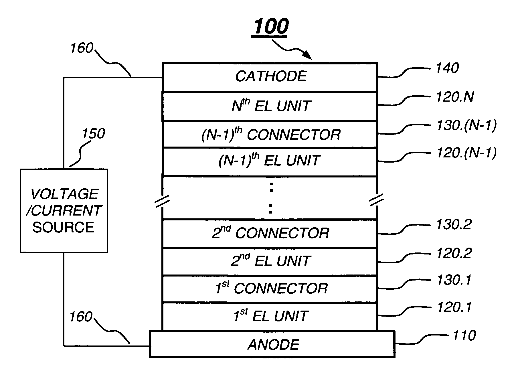
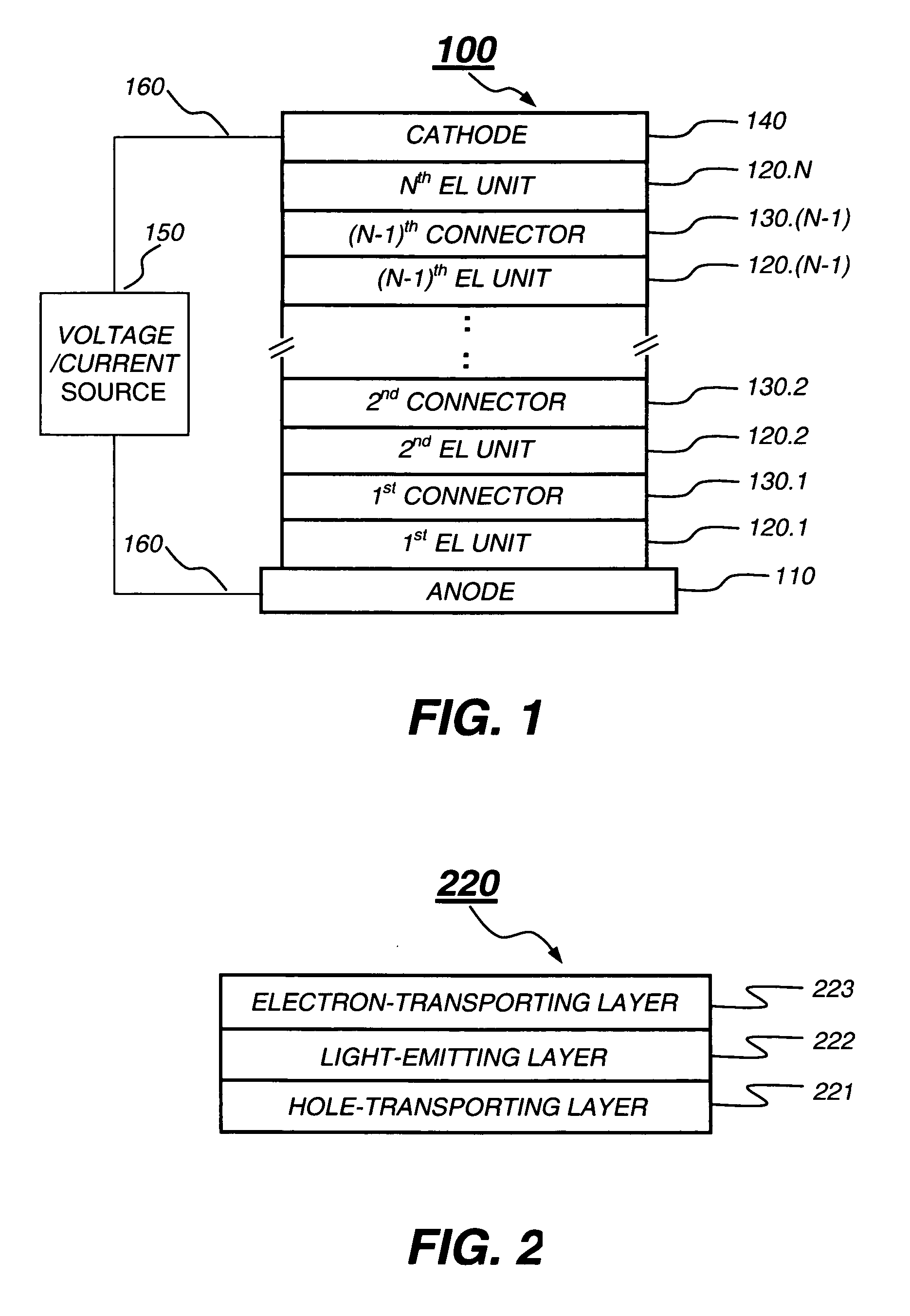
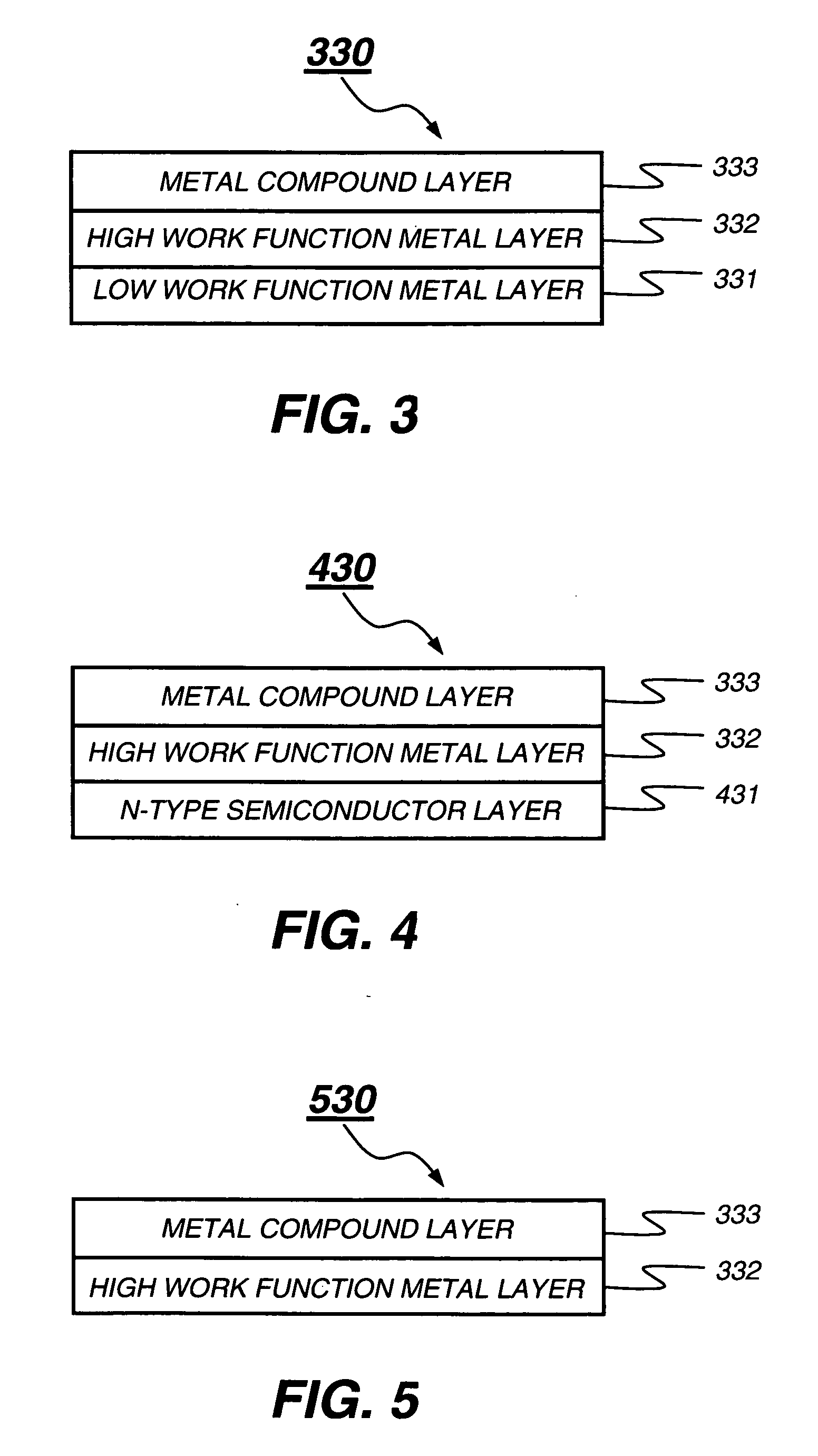
A tandem OLED includes an anode, a cathode, and a plurality of organic electroluminescent units disposed between the anode and the cathode, wherein each organic electroluminescent unit includes at least one light-emitting layer, and an intermediate connector disposed between each adjacent organic electroluminescent unit, wherein the intermediate connector includes at least a high work function metal layer having a work function of no less than 4.0 eV and a metal compound layer, wherein the intermediate connector has a sheet resistance of higher than 100 kΩ per square, and wherein the high work function metal layer improves the operational stability of the OLED.

Description

CROSS REFERENCE TO RELATED APPLICATIONS [0001] Reference is made to commonly assigned U.S. patent application Ser. No. 10 / 437,195 filed May 13, 2003 entitled “Cascaded Organic Electroluminescent Device Having Connecting Units with n-Type and p-Type Organic Layers” by Liao et al., the disclosure of which is herein incorporated by reference.FIELD OF INVENTION [0002] The present invention relates to providing a plurality of organic electroluminescent (EL) units to form a tandem (or cascaded, or stacked) organic electroluminescent device. BACKGROUND OF THE INVENTION [0003] Organic electroluminescent (EL) devices, or organic light-emitting diodes (OLEDs), are electronic devices that emit light in response to an applied potential. The structure of an OLED comprises, in sequence, an anode, an organic EL medium, and a cathode. The organic EL medium disposed between the anode and the cathode is commonly comprised of an organic hole-transporting layer (HTL) and an organic electron-transportin...

Claims


Application Information

Patent Timeline
Patent Type & Authority Applications(United States)
IPC IPC(8): H05B33/00H10K99/00
CPCH01L2251/558H01L51/5278H10K50/19H10K2102/351
Inventor LIAO, LIANG-SHENGTANG, CHING W.
Owner GLOBAL OLED TECH
Learn More