
CVD tantalum compounds for FET gate electrodes

a gate electrode and tantalum compound technology, applied in the field of gate materials for field effect transistors, can solve problems such as damage to the gate dielectri

Inactive Publication Date: 2005-11-10
NARAYANAN VIJAY +12
View PDF3 Cites 13 Cited by
  • Summary
  • Abstract
  • Description
  • Claims
  • Application Information

AI Technical Summary

Problems solved by technology

In addition, plasma processes can also result in damage to the gate dielectric.

Method used


Image

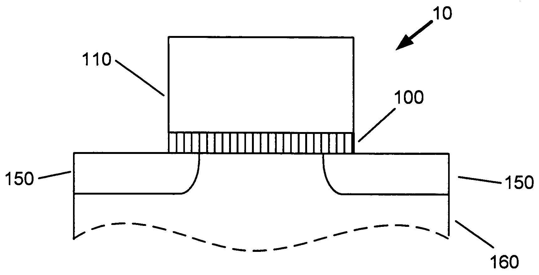
  • CVD tantalum compounds for FET gate electrodes
  • CVD tantalum compounds for FET gate electrodes
  • CVD tantalum compounds for FET gate electrodes

Examples


Embodiment Construction

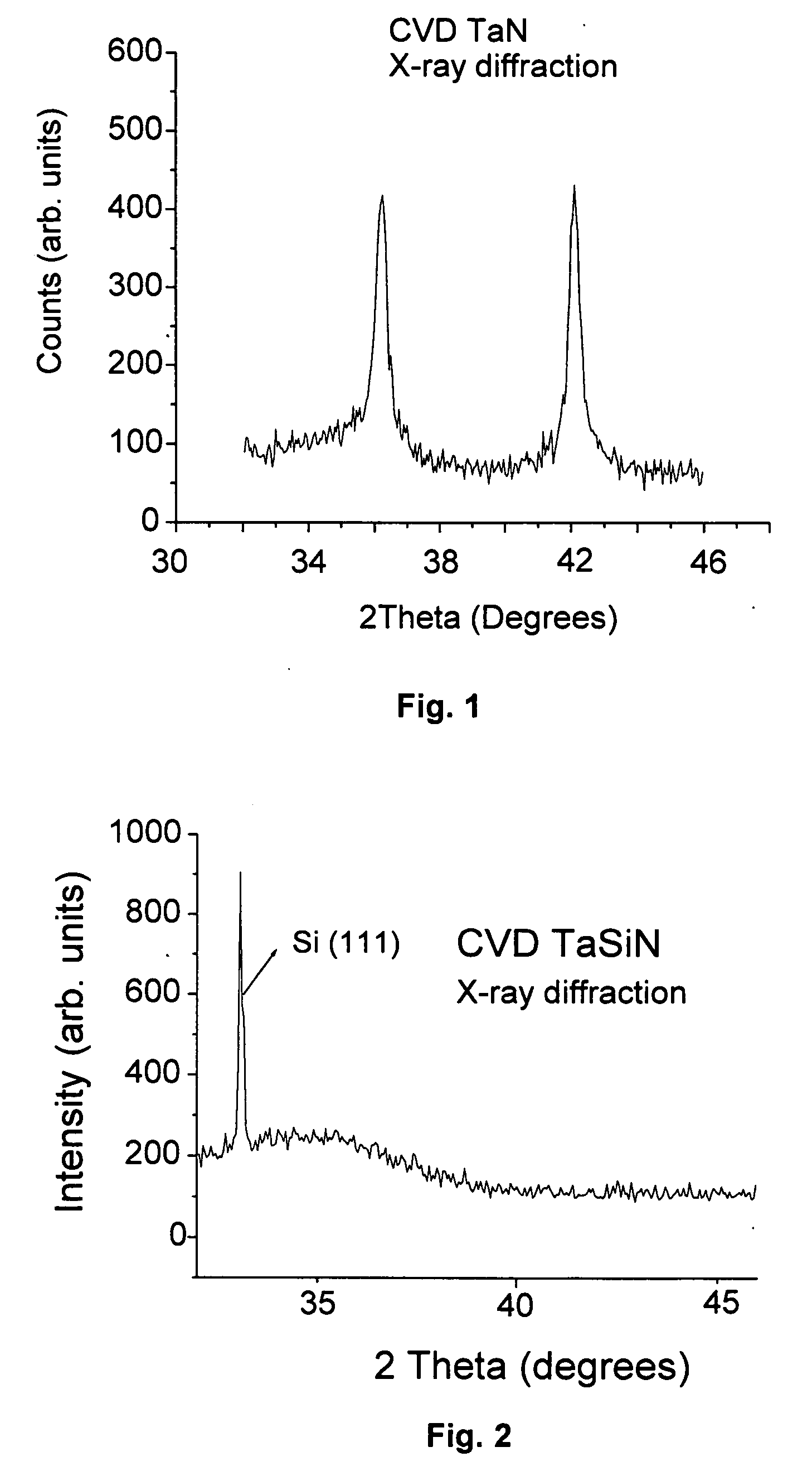
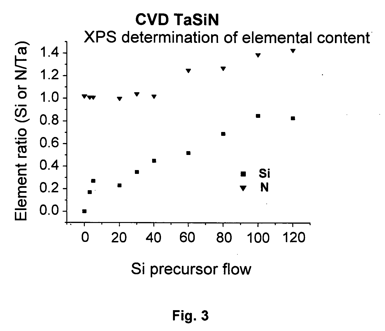
[0019] A chemical vapor deposition (CVD) processes have been developed for producing metallic tantalum (Ta)-nitrogen (N) compounds, such as TaN and TaSiN. In these processes an alkylimidotris (dialkylamido)Ta species, or material: tertiaryamylimidotris (dimethylamido)Ta (TAIMATA) was used as the Ta precursor. Ammonia (NH3) served as the source for nitrogen (N) in the CVD deposition, while hydrogen H2 was used for carrier gas. For one ordinarily skilled in the art it might be apparent that other materials could be substituted in the process for the ammonia and the hydrogen. With the tertiaryamylimidotris(dimethylamido)Ta (TAIMATA) and ammonia precursors and hydrogen carrier one obtains stoichiometric TaN, with a near 1:1 ratio of Ta to N, as determined by X-ray Photoelectron Spectroscopy (XPS). A N to Ta elemental ratio between about 0.9 and 1.1 gives layers for representative embodiments. The TaN films were deposited at a growth temperature between 400° C. and 550° C. and a chamber ...


PUM

PropertyMeasurementUnit
thicknessesaaaaaaaaaa
workfunctionaaaaaaaaaa

Abstract

Compounds of Ta and N, potentially including further elements, and with a resistivity below about 20 mΩcm and with the elemental ratio of N to Ta greater than about 0.9 are disclosed for use as gate materials in field effect devices. A representative embodiment of such compounds, TaSiN, is stable at typical CMOS processing temperatures on SiO2 containing dielectric layers and high-k dielectric layers, with a workfunction close to that of n-type Si. Metallic Ta—N compounds are deposited by a chemical vapor deposition method using an alkylimidotris(dialkylamido)Ta species, such as tertiaryamylimidotris(dimethylamido)Ta (TAIMATA), as Ta precursor. The deposition is conformal allowing for flexible introduction of the Ta—N metallic compounds into a CMOS processing flow. Devices processed with TaN or TaSiN show near ideal characteristics.

Description

FIELD OF THE INVENTION [0001] The present invention relates to a new class of gate materials for field effect transistors allowing better device properties and expanded device choices in the deeply submicron regime. More specifically, the invention teaches MOS gates formed with metallic tantalum-nitrogen compounds. BACKGROUND OF THE INVENTION [0002] Today's integrated circuits include a vast number of devices. Smaller devices are key to enhance performance and to improve reliability. As MOSFET (Metal Oxide Semiconductor Field-Effect-Transistor, a name with historic connotations meaning in general an insulated gate Field-Effect-Transistor) devices are being scaled down, the technology becomes more complex and new methods are needed to maintain the expected performance enhancement from one generation of devices to the next. [0003] Some of the requirements for the gate of a MOSFET are the following: it has to be a conductor; it has to fit into a device fabrication process, namely that ...

Claims


Application Information

Patent Timeline
Patent Type & Authority Applications(United States)
IPC IPC(8): C23C16/34H01L21/28H01L21/336H01L21/8234H01L21/8238H01L29/10H01L29/49H01L29/772H01L29/78
CPCC23C16/34H01L21/28088H01L29/78H01L29/4966H01L21/823828H01L21/18H01L21/8234H01L21/8238
Inventor NARAYANAN, VIJAYMCFEELY, FENTON R.MILKOVE, KEITH RAYMONDYURKAS, JOHN JACOBCOPEL, MATTHEW WARRENJAMISON, PAUL CHARLESCARRUTHERS, ROY A.CABRAL, CYRIL JR.SIKORSKII, EDMUND M.DUCH, ELIZABETH A.CALLEGARI, ALESSANDRO C.ZAFAR, SUFINAKAMURA, KAZUHITO
Owner NARAYANAN VIJAY
Learn More