Method for fabricating semiconductor device having trench isolation
- Summary
- Abstract
- Description
- Claims
- Application Information
AI Technical Summary
Benefits of technology
Problems solved by technology
Method used
Image
Examples
Embodiment Construction
[0029] A method for fabricating a semiconductor device having a trench-shaped layer for isolating device elements in accordance with a preferred embodiment of the present invention will be described in detail with reference to the accompanying drawings.
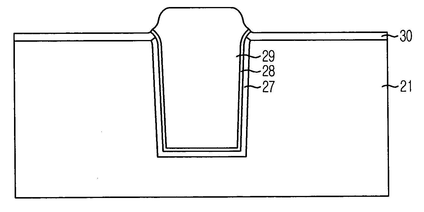
[0030]FIGS. 2A to 2H are cross-sectional views illustrating a method for fabricating a semiconductor device having a trench shaped layer for isolating device elements in accordance with a preferred embodiment of the present invention.
[0031] Referring to FIG. 2A, a pad oxide layer 22 and a pad nitride layer 23 are sequentially formed on a silicon substrate 21. Herein, the pad nitride layer 23 serves a role of an etch barrier layer later and a polishing stop layer during a subsequent chemical mechanical polishing (CMP) process. Preferably, the pad oxide layer 22 should be a silicon oxide (SiO2) layer with a thickness ranging from 50 Å to 300 Å and the pad nitride layer 23 should be a silicon nitride (Si3N4) layer with a thickness rang...
PUM
 Abstract
Description
Claims
Application Information
 - R&D Engineer
- R&D Manager
- IP Professional
- Industry Leading Data Capabilities
- Powerful AI technology
- Patent DNA Extraction
Browse by: Latest US Patents, China's latest patents, Technical Efficacy Thesaurus, Application Domain, Technology Topic, Popular Technical Reports.
© 2024 PatSnap. All rights reserved.Legal|Privacy policy|Modern Slavery Act Transparency Statement|Sitemap|About US| Contact US: help@patsnap.com


