Operation scheme for programming charge trapping non-volatile memory
- Summary
- Abstract
- Description
- Claims
- Application Information
AI Technical Summary
Benefits of technology
Problems solved by technology
Method used
Image
Examples
Embodiment Construction
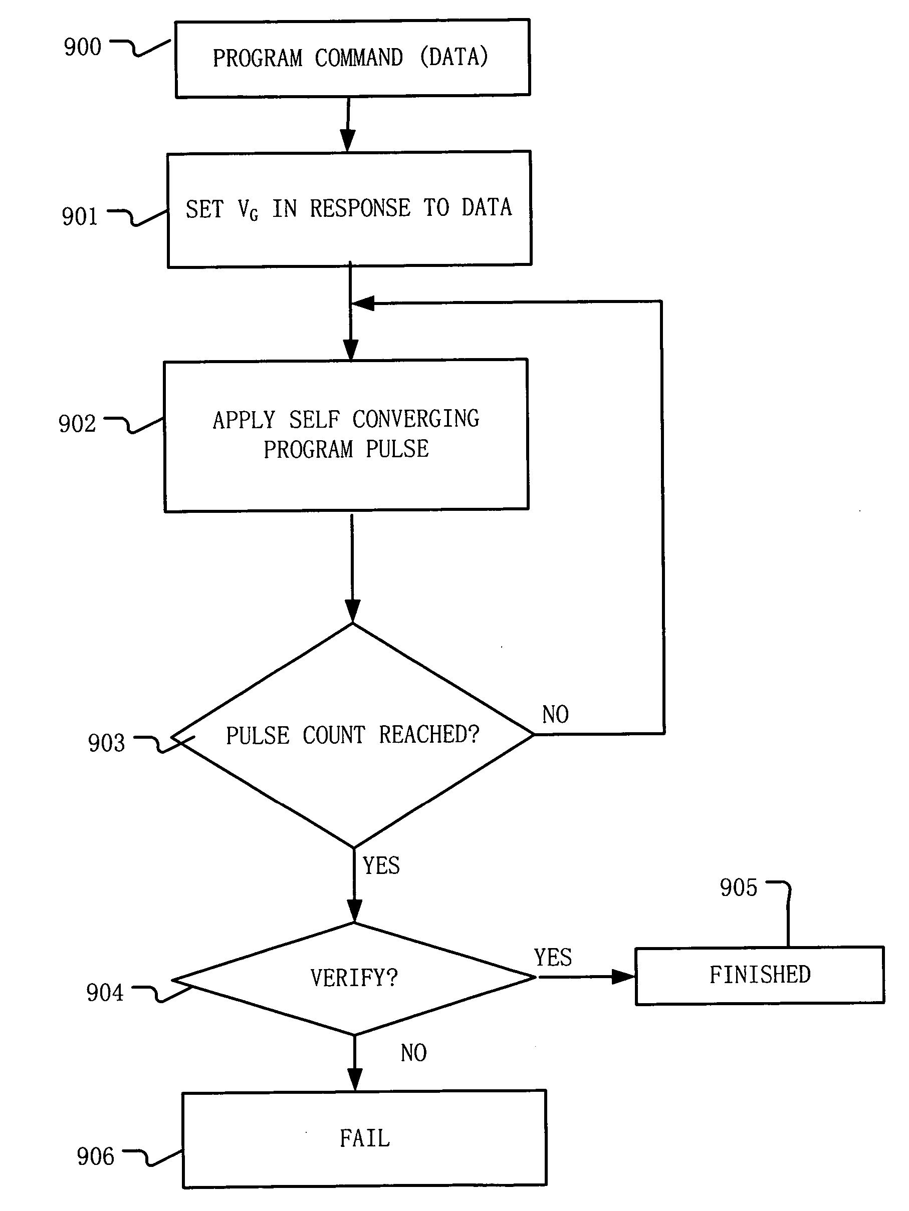
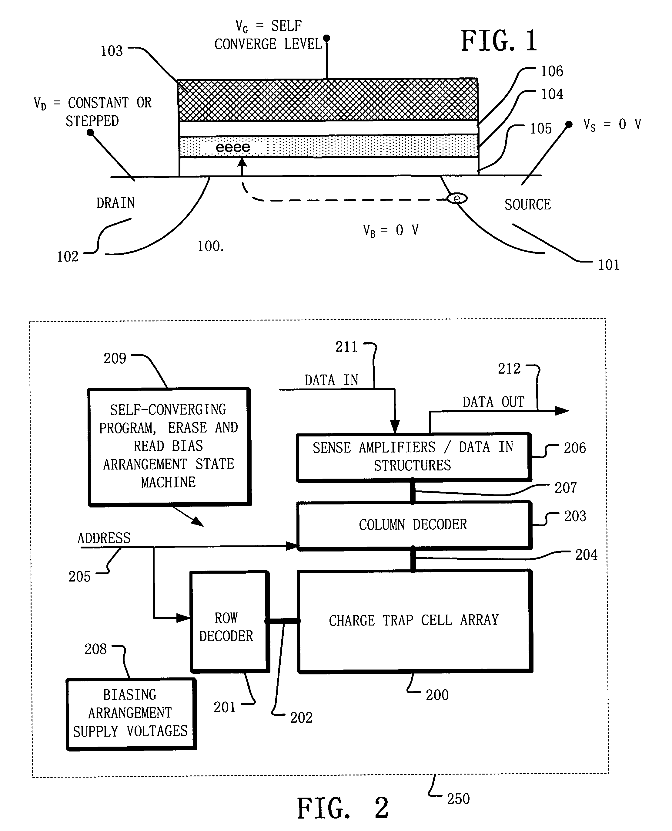
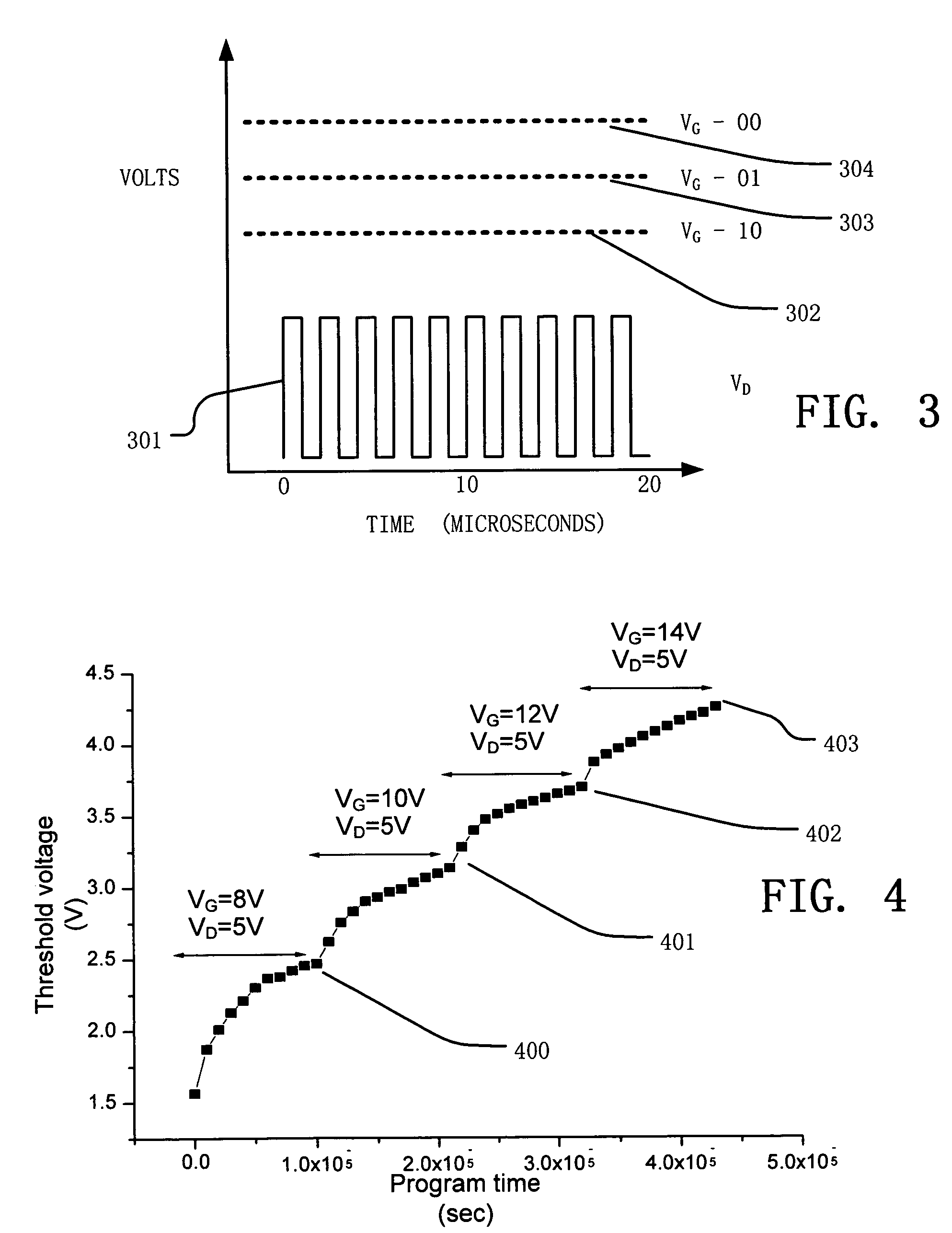
[0032] A detailed description of embodiments of the present invention is provided with reference to FIGS. 1-10.
[0033]FIG. 1 is a simplified diagram of an NROM memory cell suitable for use in embodiments of the present invention. The memory cell is implemented in a semiconductor substrate 100. The cell includes a source 101 and a drain 102 formed by respective diffusion regions, separated by a channel in the substrate 100. A control gate 103 overlies the channel. A charge storage element, such as charge trapping layer 104, is isolated by an insulator 106 such as silicon dioxide or silicon oxynitride between the charge trapping layer 104 and the control gate 103 and an insulator, such as gate dielectric 105 comprising silicon dioxide or silicon oxynitride between the charge trapping layer 104 and the channel. The charge trapping layer 104 comprises silicon nitride or silicon oxynitride in typical NROM cells. In other embodiments, other charge trapping material, such as Al2O3, HfOx, Z...
PUM
 Abstract
Description
Claims
Application Information
 - R&D
- Intellectual Property
- Life Sciences
- Materials
- Tech Scout
- Unparalleled Data Quality
- Higher Quality Content
- 60% Fewer Hallucinations
Browse by: Latest US Patents, China's latest patents, Technical Efficacy Thesaurus, Application Domain, Technology Topic, Popular Technical Reports.
© 2025 PatSnap. All rights reserved.Legal|Privacy policy|Modern Slavery Act Transparency Statement|Sitemap|About US| Contact US: help@patsnap.com


