
Image capture apparatus

a technology of image capture and apparatus, applied in the direction of color television details, semiconductor devices, television systems, etc., can solve the problems of difficult to precisely position these devices or members, complicated assembly process, and difficult to precisely determine the relative positions of solid state imaging devices and taking lenses

Inactive Publication Date: 2005-09-29
FUJIFILM CORP
View PDF13 Cites 54 Cited by
  • Summary
  • Abstract
  • Description
  • Claims
  • Application Information

AI Technical Summary

Benefits of technology

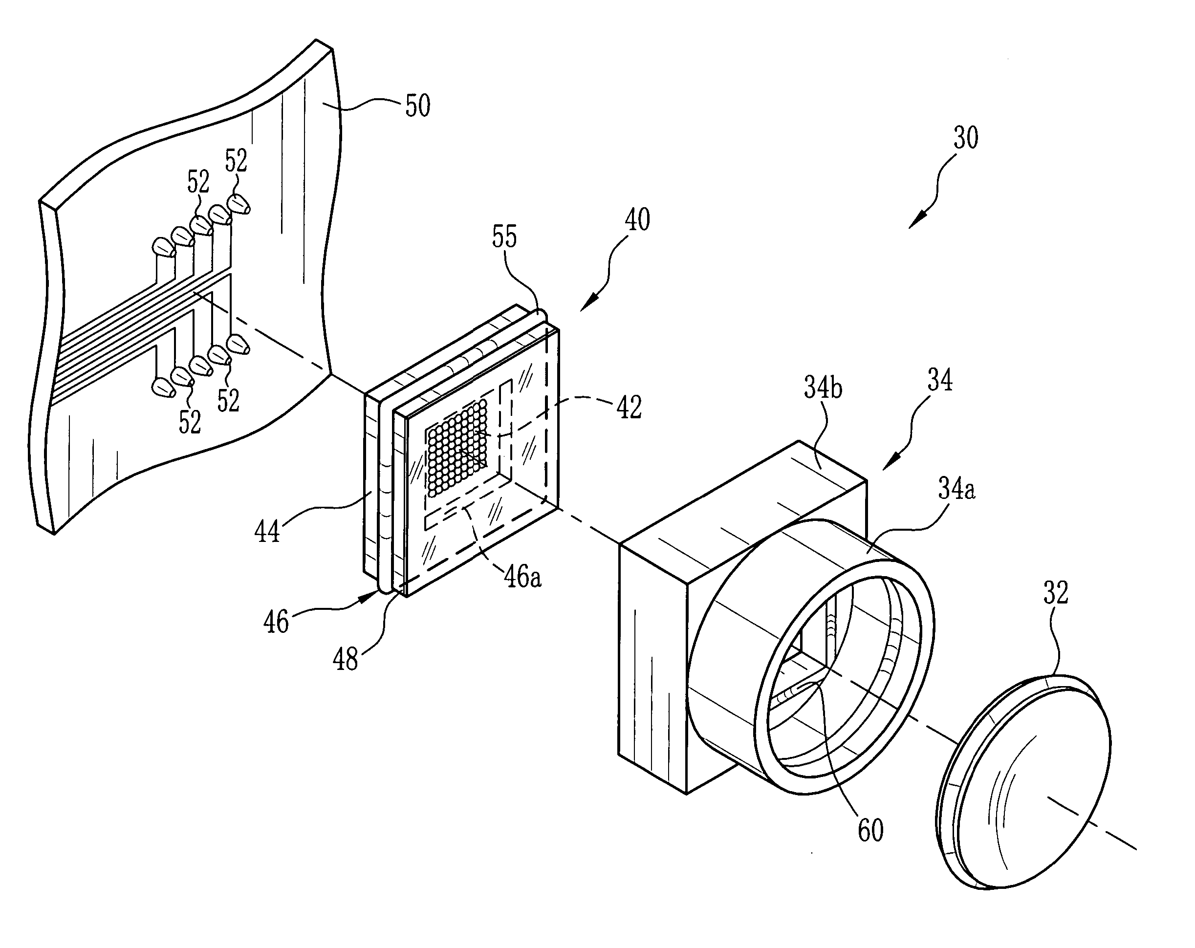
The present invention provides an image capture apparatus that is easy to assemble with precision and prevents damage to the solid state imaging device and taking lens from external force such as impact shock. The apparatus includes a lens holding frame with a projection and a groove for fitting the solid state imaging device. A protector covers the lens holding frame and a shock absorber is placed between the protector and the lens holding frame. The projection and groove fit together to secure the solid state imaging device, and the apparatus is assembled with higher accuracy. The manufacturing cost can be held down by adjusting the size of the projection and groove.

Problems solved by technology

However, when it is designed to adhere the solid state imaging device to the lens holding frame, it is difficult to precisely position these devices or members.
Further, to use the pair of lens holding frames as described in Japanese Patent Laid-Open Publications No.08-307744, complicated assembling process is needed.
In addition, in Japanese Patent Laid-Open Publications No.2002-185826, it is difficult to precisely determine relative positions of the solid state imaging device and the taking lens, because the solid state imaging device is mounted on the subsidiary substrate, and both the subsidiary substrate and the lens holding frame are attached on the main substrate.
It is difficult to precisely set all these members at their correct positions.

Method used


Image

  • Image capture apparatus
  • Image capture apparatus
  • Image capture apparatus

Examples


Embodiment Construction

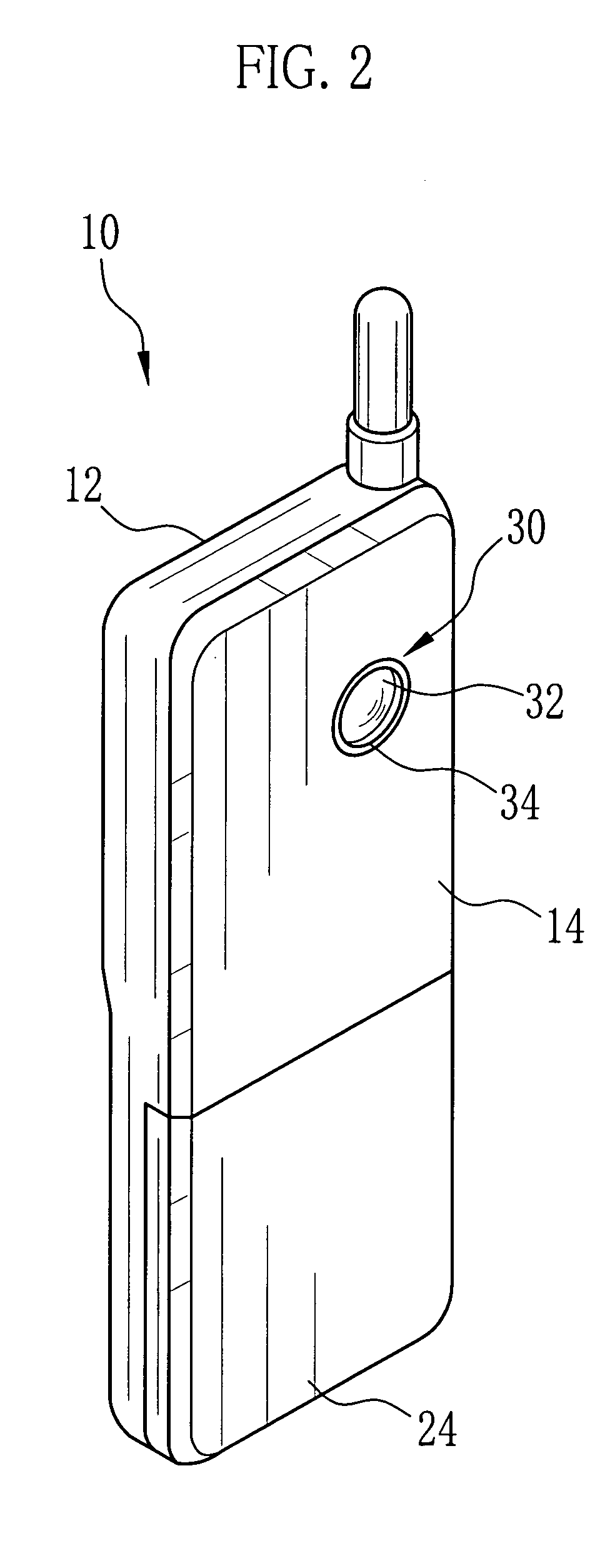
[0026] In FIG. 1 and FIG. 2, a mobile phone with a camera 10 has an outer package constituted of a front cover 12 and a rear cover 12. A circuit board on which electronic components are provided is contained within these covers. In a front face of the mobile phone 10, there are an operation section 16, liquid-crystal display panel 18, an ear receiver 20 and a microphone 22, while the ear receiver 20 and the microphone 22 are used for conversation. In the mobile phone 10, a battery 24 for supplying electric power is attached to a rear face thereof in a detachable manner, and an image capture apparatus 30 having a taking lens 32 and a lens holding frame 34 is disposed.

[0027] The mobile phone with a camera 10 operates in a telephone mode for having a conversation through the ear receiver 20 and the microphone 22, and in a camera mode for storing images through the taking lens 32 in an internal memory (not shown). These modes can be switched by operating the operation section 16. In ad...


PUM


Abstract

A solid state imaging device is consisted of an image sensor chip having a light receiving portion, a frame-like spacer attached on the image sensor chip so as to surround the light receiving portion, and a transparent cover glass attached on the spacer so as to close the light receiving portion. An outer periphery of the spacer is projected from that of the solid state imaging device to form a projection. Along an inner periphery of a lens holding frame, a groove is formed. When the lens holding frame is attached to the solid state imaging device to cover it, the groove of the lens holding frame is engaged to the projection of the solid state imaging device.

Description

BACKGROUND OF THE INVENTION [0001] 1. Field of the Invention [0002] The present invention relates to an image capture apparatus used in an electronic camera, a mobile phone and so on. [0003] 2. Description Related to the Prior Art [0004] An image capture apparatus, for example a digital camera and a digital video camera, using a solid state imaging device (such as CCDs, CMOS type and the like) is in widespread use. Further, an electronic apparatus (a personal computer, a mobile phone, an electronic notepad or the like) is provided with the image capture apparatus, to have an image-taking function. [0005] In packaging methods for the solid state imaging device, there is a ceramic packaging method. In this method, an image sensor chip on which light receiving portion is formed is mounted on a subsidiary substrate, then a ceramic frame is disposed on the subsidiary substrate so as to surround the image sensor chip, and then a transparent plate is disposed on the ceramic frame so as to ...

Claims


Application Information

Patent Timeline
Patent Type & Authority Applications(United States)
IPC IPC(8): H04N5/225H01L27/14
CPCH04N5/2254H01L27/14618H04N23/55
Inventor SATO, TSUNEOISHIHARA, ATSUHIKOYAMASAKO, HIROSHISAWACHI, YOUICHIKIUCHI, TAKAOIWATA, NAOYA
Owner FUJIFILM CORP
Learn More