
Subwavelength-diameter silica wires for low-loss optical waveguiding

a technology of optical waveguided wires and subwavelength diameters, which is applied in the manufacture of instruments, cladded optical fibres, manufacturing tools, etc., can solve the problems of difficult to draw smnws with uniform diameters, impractical laser power requirements, and difficult to manufacture such silica wires, etc., to achieve the effect of softening the fiber portion

Inactive Publication Date: 2005-09-22
PRESIDENT & FELLOWS OF HARVARD COLLEGE
View PDF21 Cites 25 Cited by
  • Summary
  • Abstract
  • Description
  • Claims
  • Application Information

AI Technical Summary

Benefits of technology

[0011] In another aspect, the size of the portion of the support element coupled to the preform and its distance from the heated portion of the support element, together with judicious selection of the material forming the support element, allow the portion coupled to the preform to function as a thermal reservoir element that ensures a steady temperature distribution across the drawing region by reducing the rate of transfer of temporal fluctuations in the temperature of the heated portion to the drawing region.
[0012] In one aspect, the support element can be a tapered sapphire rod extending from a base portion to a tip portion to which the silica preform can be coupled. For example, the silica preform can be wrapped around the tip portion while the tip portion is heated, for example, by placing a selected segment of the sapphire rod in a flame. The tip portion is preferably heated to a temperature that is sufficiently high to cause softening of the preform, thereby facilitating its coupling to the support element. Subsequently, the preform can be drawn to generate the nano-sized silica fiber.
[0019] In yet another aspect, the invention provides a method of forming a nano-sized fiber that includes the steps of thermally coupling a proximal portion of a silica fiber having a diameter in a range of about 1 to about 20 microns to a tip portion of a thermally conductive support element such that another portion of the fiber extends vertically down from the tip portion of the support element. The support element can be heated at a selected distance from the tip portion so as to raise the temperature of the tip portion (e.g., to a temperature in a range of about 1500 C to about 1800 C) so as to soften the fiber portion coupled to the support element. A gravitational pull generated by the vertically extending fiber portion causes drawing of the fiber into a wire having a diameter in a range of about 20 nm to about 1000 nm.

Problems solved by technology

Although photonic applications can benefit from incorporation of silica submicrometer- or nanometer-diameter wires (SMNW), the fabrication of such silica wires presents a number of challenging problems.
In particular, both theoretical and experimental results indicate that the laser power required for drawing silica SMNWs with a uniform diameter from a laser-heated melt is impractically large.
Further, it is difficult to draw SMNWs having uniform diameters from a flame-heated melt because turbulence and convention render controlling the temperature gradient in the drawing region problematical.
Moreover, silica nanowires obtained recently by employing other methods exhibit large diameter fluctuations and sidewall roughness that render these wires unsuitable for low-loss optical waveguiding.

Method used


Image

  • Subwavelength-diameter silica wires for low-loss optical waveguiding
  • Subwavelength-diameter silica wires for low-loss optical waveguiding
  • Subwavelength-diameter silica wires for low-loss optical waveguiding

Examples


Embodiment Construction

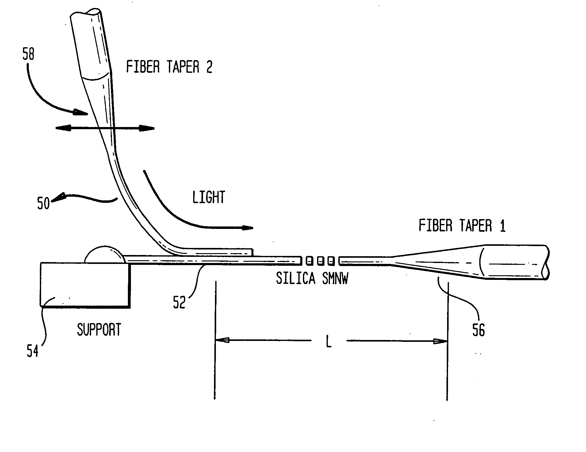
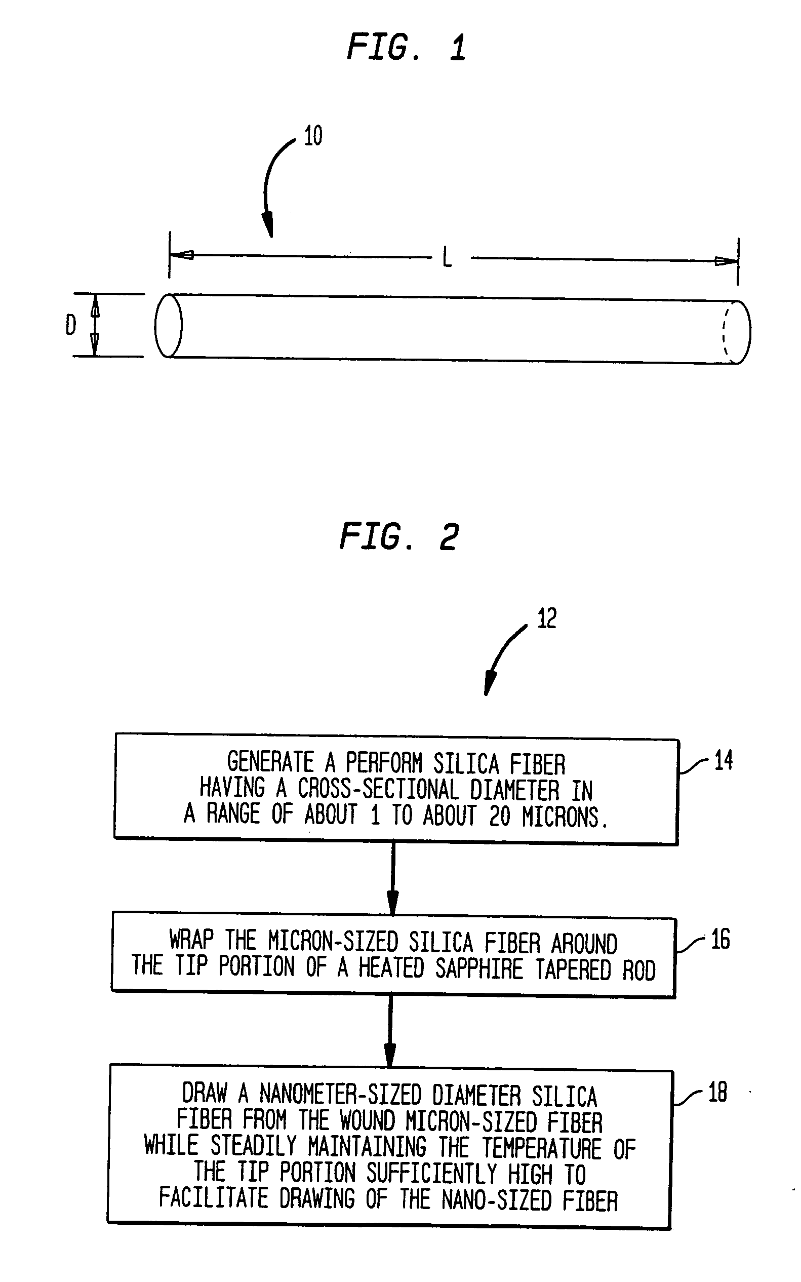
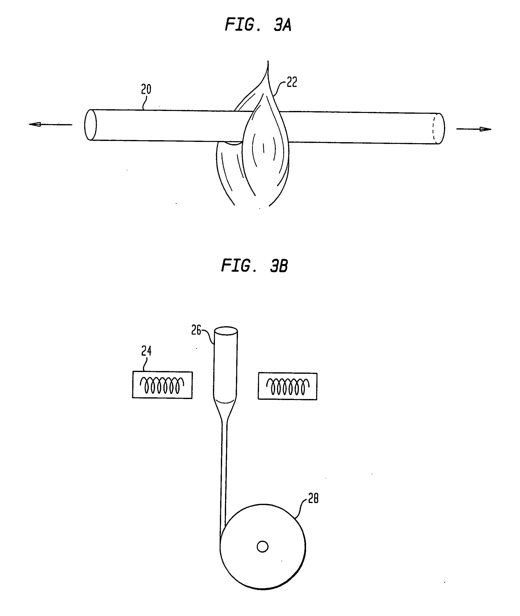
[0064] The present invention provides nanometer-sized diameter silica fibers, and methods for their production, that exhibit a high uniformity in diameter size along the fiber's length as well as a highly smooth surface with a root mean square roughness that can be less than about 0.5 nm. As discussed in more detail below, an exemplary method of the invention for generating such silica fibers utilizes a process in which a silica fiber preform having a micrometer-sized diameter is thermally coupled to a portion of a support element. The support element is heated so as to maintain the fiber at a temperature that allows drawing the preform in a subsequent step to form a nanometer-sized diameter silica fiber.

[0065]FIG. 1 schematically depicts an exemplary silica fiber 10, formed in accordance with the teachings of the invention, that exhibits a cross-sectional diameter D with a value in a range of about 50 nm to about 1100 nm, or in some preferred embodiments in a range of about 20 nm ...


PUM

PropertyMeasurementUnit
Lengthaaaaaaaaaa
Diameteraaaaaaaaaa
Diameteraaaaaaaaaa

Abstract

The present invention provides nanometer-sized diameter silica fibers that exhibit high diameter uniformity and surface smoothness. The silica fibers can have diameters in a range of a about 20 nm to about 1000 nm. An exemplary method according to one embodiment of the invention for generating such fibers utilizes a two-step process in which in an initial step a micrometer sized diameter silica preform fiber is generated, and in a second step, the silica preform is drawn while coupled to a support element to form a nanometer sized diameter silica fiber. The portion of the support element to which the preform is coupled is maintained at a temperature suitable for drawing the nansized fiber, and is preferably controlled to exhibit a temporally stable temperature profile.

Description

RELATED APPLICATION [0001] This application claims priority to a provisional application entitled “Subwavelength-diameter silica wires for low-loss optical waveguiding” having a Ser. No. 60 / 530467 and filed on Dec. 16, 2003.FEDERALLY SPONSORED RESEARCH [0002] The invention was made with Government support under contract PHY-0117795 awarded by National Science Foundation (NSF). The Government has certain rights in the invention.BACKGROUND OF THE INVENTION [0003] The present invention relates generally to silica wires having sub-micrometer or nanometer-sized diameters, and methods for forming such wires, and more particularly, to fabrication methods that provide nano-sized silica wires having enhanced uniformity and surface smoothness. [0004] Miniature silica waveguides with diameters or widths larger than the wavelength of transmitted light are widely utilized in optical communications, sensors, and other applications. Silica wires with diameters more than one micrometer, which allow...

Claims


Application Information

Patent Timeline
IPC IPC(8): C03B37/025C03B37/027C03B37/15G02B6/02G02B6/08G02B6/10G02B6/12G02B6/255G02B6/28
CPCB82Y20/00C03B37/025C03B37/027C03B37/15G02B6/2835C03B2201/34G02B6/107G02B6/2552C03B2201/02
Inventor MAZUR, ERICTONG, LIMINGATTASS, RAFAEL
Owner PRESIDENT & FELLOWS OF HARVARD COLLEGE
Learn More