
Non-volatile memory with synchronous DRAM interface

a non-volatile memory and interface technology, applied in the field of memory devices, can solve the problems of prohibitive use of nand architecture flash memory for large numbers of non-sequential individual data word accesses, difficult to correct individual errors in arrays, etc., and achieve the effect of high density non-volatile memory, easy access, and simplified use and design effor

Inactive Publication Date: 2005-09-15
MICRON TECH INC
View PDF20 Cites 213 Cited by
  • Summary
  • Abstract
  • Description
  • Claims
  • Application Information

AI Technical Summary

Benefits of technology

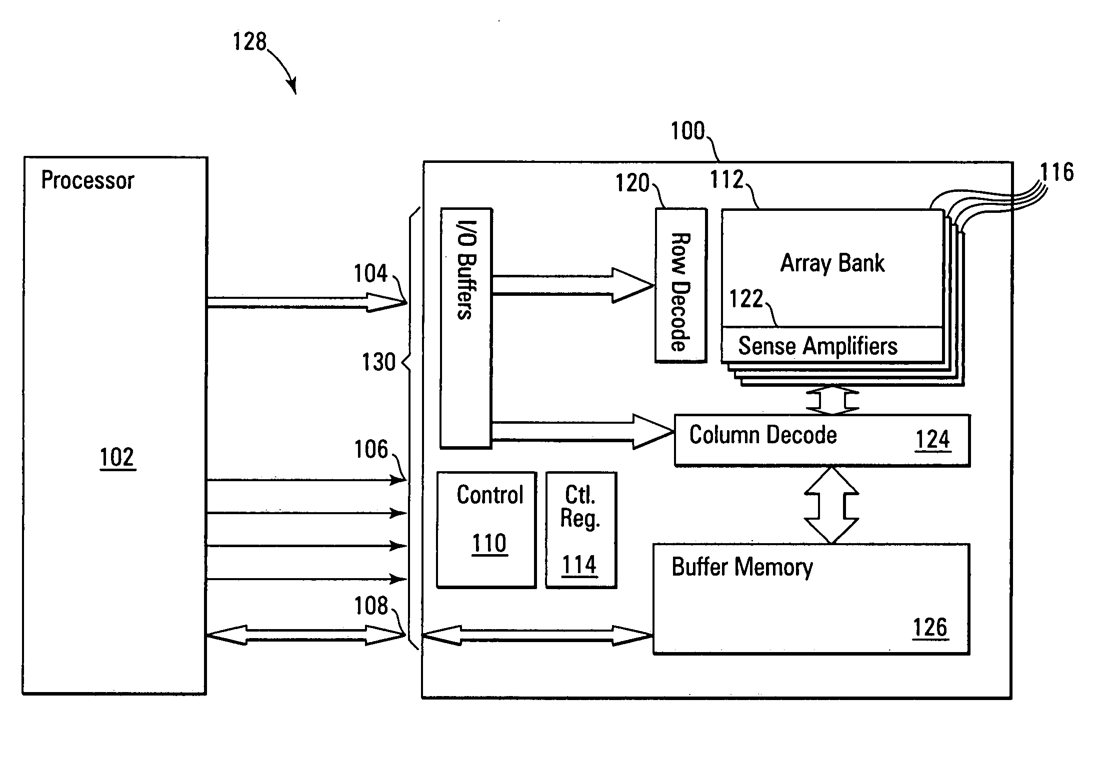
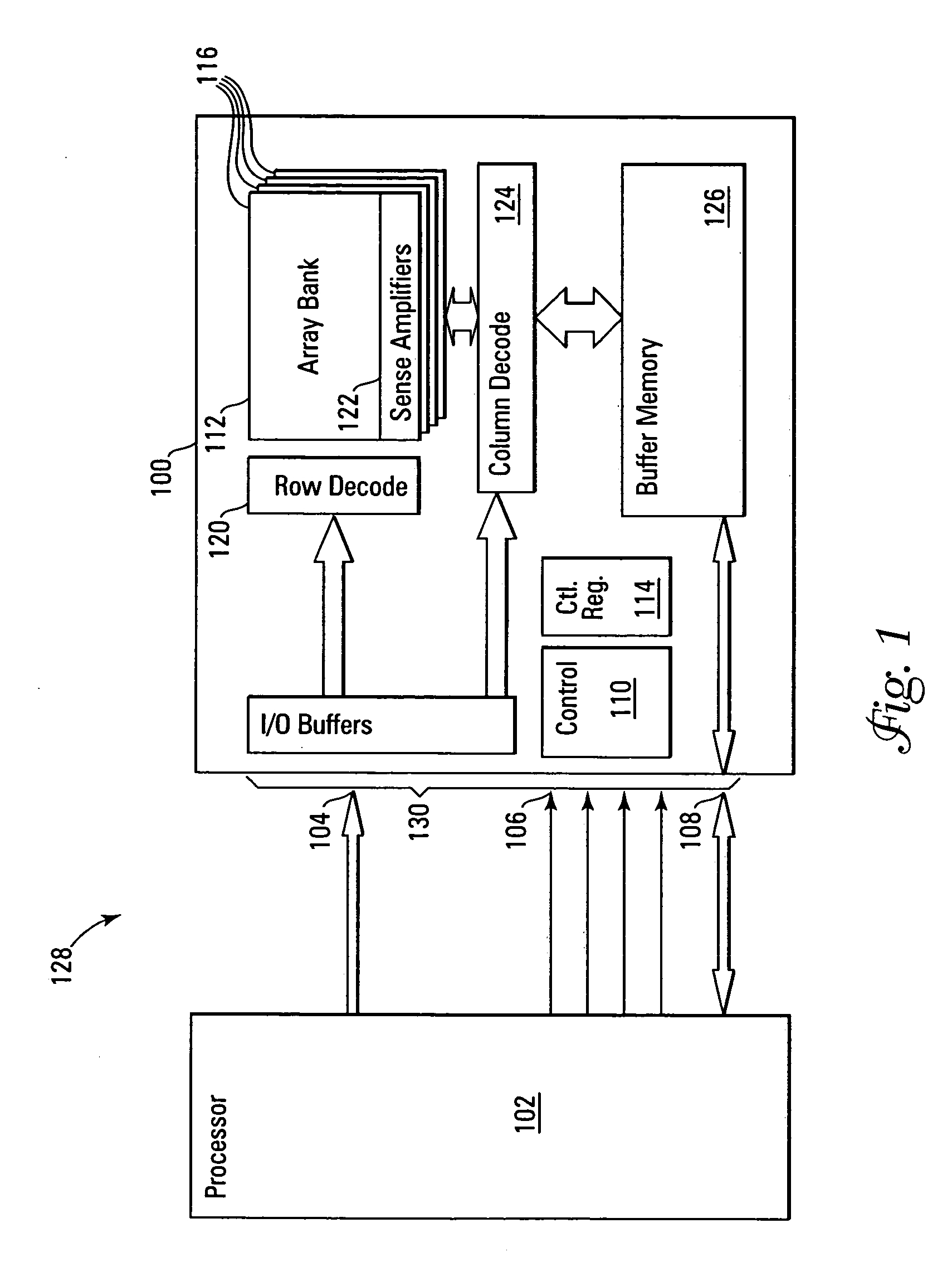
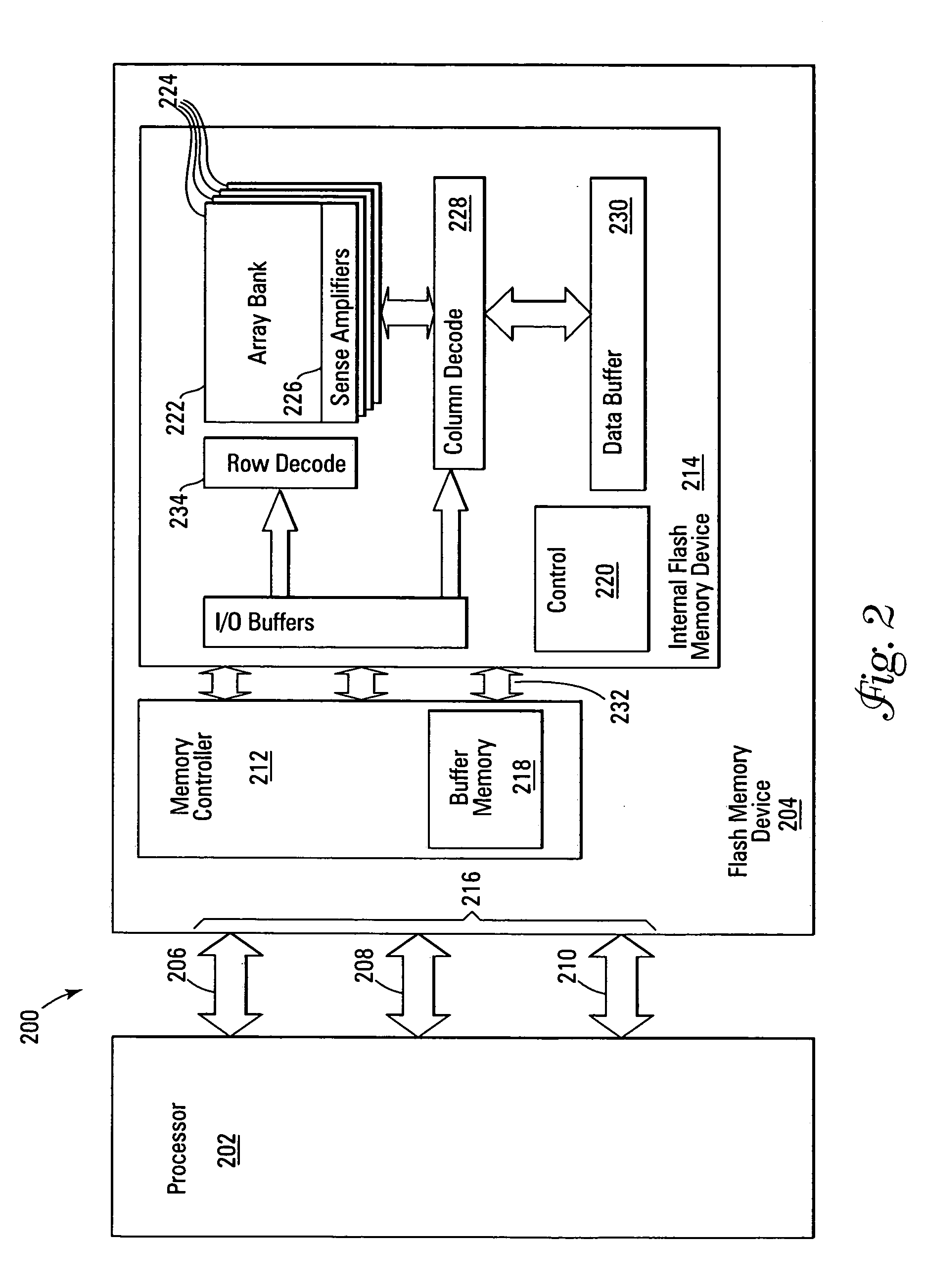
[0011] Although described in relation to NAND architecture Flash memory, the various embodiments relate generally to non-volatile memory devices and subsystems that incorporate a synchronous interface. Memory device embodiments of the present invention utilize an external or embedded controller and / or memory buffer to present the non-volatile memory device(s) as a conventional memory device having a synchronous interface. This allows the non-volatile memory embodiments of the present invention to support in-place code execution and allow them to be booted from. Additionally, the memory buffer allows for caching / buffering of data read and / or write accesses, allowing non-volatile memory devices of the present invention to be quickly accessed as if they were conventional synchronous RAM memory devices.
[0012] In one embodiment of the present invention, a non-volatile memory device eliminates the requirement of external drivers, customized NAND interface port on a memory controller or microprocessor, and / or operating system support to utilize a specialized high density non-volatile memory device, and in particular, a NAND architecture Flash memory device. This simplifies the use and design effort of high density non-volatile memories by reducing specialized interfacing, while reducing the overall production cost through allowing use of a less expensive NAND architecture Flash memory or other high density non-volatile memory where a more expensive memory device would normally be required. In another embodiment of the present invention, a NAND architecture Flash card or subsystem has a synchronous interface. In a further embodiment of the present invention, a NAND architecture Flash memory device, card, or subsystem has an SDRAM compatible interface. In yet a further embodiment of the present invention, individual data words of a NAND architecture Flash memory device, card, or subsystem may be accessed in a non-prohibitive manner. In another embodiment of the present invention, a NAND architecture Flash memory device, card, or subsystem is accessed by a row and column address. In yet another embodiment of the present invention, a NAND architecture Flash memory device, card, or subsystem contains a RAM buffer allowing in-place code execution and / or read / write access.

Problems solved by technology

Most RAM is volatile, which means that it requires a steady flow of electricity to maintain its contents.
A problem with NAND Flash memory is that with its higher density and configuration it requires specialized interfacing and interaction to utilize; many available processors and memory controllers do not directly support NAND Flash memory whereas NOR Flash memory support is more commonly available.
Typically this means that a majority of the control and management of a NAND Flash memory device is external from the memory device and in expensive dedicated hardware or a software driver that is executed on a coupled memory controller or processor.
In addition, as multiple floating gate memory cell transistors are coupled together in the strings of a NAND Flash memory array, individual errors in the array are more difficult to correct for than in NOR Flash memory.
This issue becomes even more of a problem when multi-level memory cells (MLCs), which store multiple memory states in each cell, are utilized.
These features make the use of NAND architecture Flash memories for large numbers of non-sequential individual data word accesses prohibitive.
SDRAM's can be accessed quickly, but are volatile.

Method used


Image

  • Non-volatile memory with synchronous DRAM interface
  • Non-volatile memory with synchronous DRAM interface
  • Non-volatile memory with synchronous DRAM interface

Examples


Embodiment Construction

[0022] In the following detailed description of the invention, reference is made to the accompanying drawings that form a part hereof, and in which is shown, by way of illustration, specific embodiments in which the invention may be practiced. In the drawings, like numerals describe substantially similar components throughout the several views. These embodiments are described in sufficient detail to enable those skilled in the art to practice the invention. Other embodiments may be utilized and structural, logical, and electrical changes may be made without departing from the scope of the present invention. The following detailed description is, therefore, not to be taken in a limiting sense, and the scope of the present invention is defined only by the appended claims and equivalents thereof.

[0023] Although described in relation to NAND architecture Flash memory, the various embodiments relate generally to non-volatile memory devices and subsystems that incorporate a synchronous i...


PUM


Abstract

A high density non-volatile memory system, card, and device is described that incorporates a synchronous interface. This is accomplished through use of an external or embedded controller and / or memory buffer to manage the high density non-volatile memory device(s) to present it as a conventional memory device having a synchronous interface that is accessible by row and column address. This allows the high density non-volatile memory to support in-place code execution and allows it to be booted from. Additionally, this incorporation eliminates the overhead of drivers and / or operating system support required to utilize and present conventional high density non-volatile memory devices and moves it internal to the memory device. This simplifies the use and design effort in the overhead and specialized interfacing of high density non-volatile memories and in particular, NAND architecture Flash memories, while reducing the production cost through use of less expensive high density non-volatile memory.

Description

TECHNICAL FIELD OF THE INVENTION [0001] The present invention relates generally to memory devices and in particular the present invention relates to non-volatile memory devices with synchronous interfaces. BACKGROUND OF THE INVENTION [0002] Memory devices are typically provided as internal storage areas in a computer. The term memory identifies data storage that comes in the form of integrated circuit chips. There are several different types of memory used in modern electronics, one common type is RAM (random-access memory). RAM is characteristically found in use as main memory in a computer environment. RAM refers to read and write memory; that is, you can both write data into RAM and read data from RAM. This is in contrast to ROM (read-only memory), which permits you only to read data. Most RAM is volatile, which means that it requires a steady flow of electricity to maintain its contents. [0003] Computers almost always contain a small amount of ROM that holds instructions for sta...

Claims


Application Information

Patent Timeline
IPC IPC(8): G06F12/00
CPCG06F12/0802G11C7/10G06F2212/2022G06F2212/1004
Inventor KILBUCK, KEVIN M.EGGLESTON, DAVID
Owner MICRON TECH INC
Learn More