
Mosgate driver integrated circuit with adaptive dead time

a driver and integrated circuit technology, applied in the field of driver circuits, can solve the problems that the ideal “anti-phase” control cannot prevent the simultaneous conduction of gated switches, and achieve the effect of minimizing the dead time between their conduction sequences

Inactive Publication Date: 2005-09-15
INFINEON TECH AMERICAS CORP
View PDF11 Cites 19 Cited by
  • Summary
  • Abstract
  • Description
  • Claims
  • Application Information

AI Technical Summary

Benefits of technology

[0007] It is an object of the present invention to provide a MOS-gated driver circuit capable of overcoming the disadvantages of prior art driver circuits described above. For this purpose, the present invention proposes a MOS-gated circuit capable of automatically controlling the dead-time in a closed loop to prevent the simultaneous conduction of the MOS-gated switches, such as MOSFETs or IGBTs. The dead-time determination is based on the status of each switch (e.g., the ability of each switch to withstand a reverse voltage before the other switch can turn on). In this manner, the shortest possible dead-time can be automatically provided. Any desired characteristic may be monitored, for example, threshold voltage, to determine when the MOS-gated device is capable of withstanding a reapplied voltage.
[0008] In one exemplary embodiment, an adaptive dead time circuit is provided for first and second series connected MOS-gated devices configured to conduct sequentially, but not simultaneously. The circuit includes first and second monitor circuits coupled to the MOS-gated devices configured to produce respective output signals in response to the measurement of a characteristic of the first and / or second MOS-gated devices related to their ability to withstand a reverse voltage. The output signals of the first and second monitor circuits are respectively connected to the gate electrodes of the MOS-gated devices to enable their turn on in response to an output signal from said first and second monitor circuits, respectively; whereby simultaneous conduction of the first and second MOS-gated devices is prevented and the dead-time between their conduction sequences is minimized.

Problems solved by technology

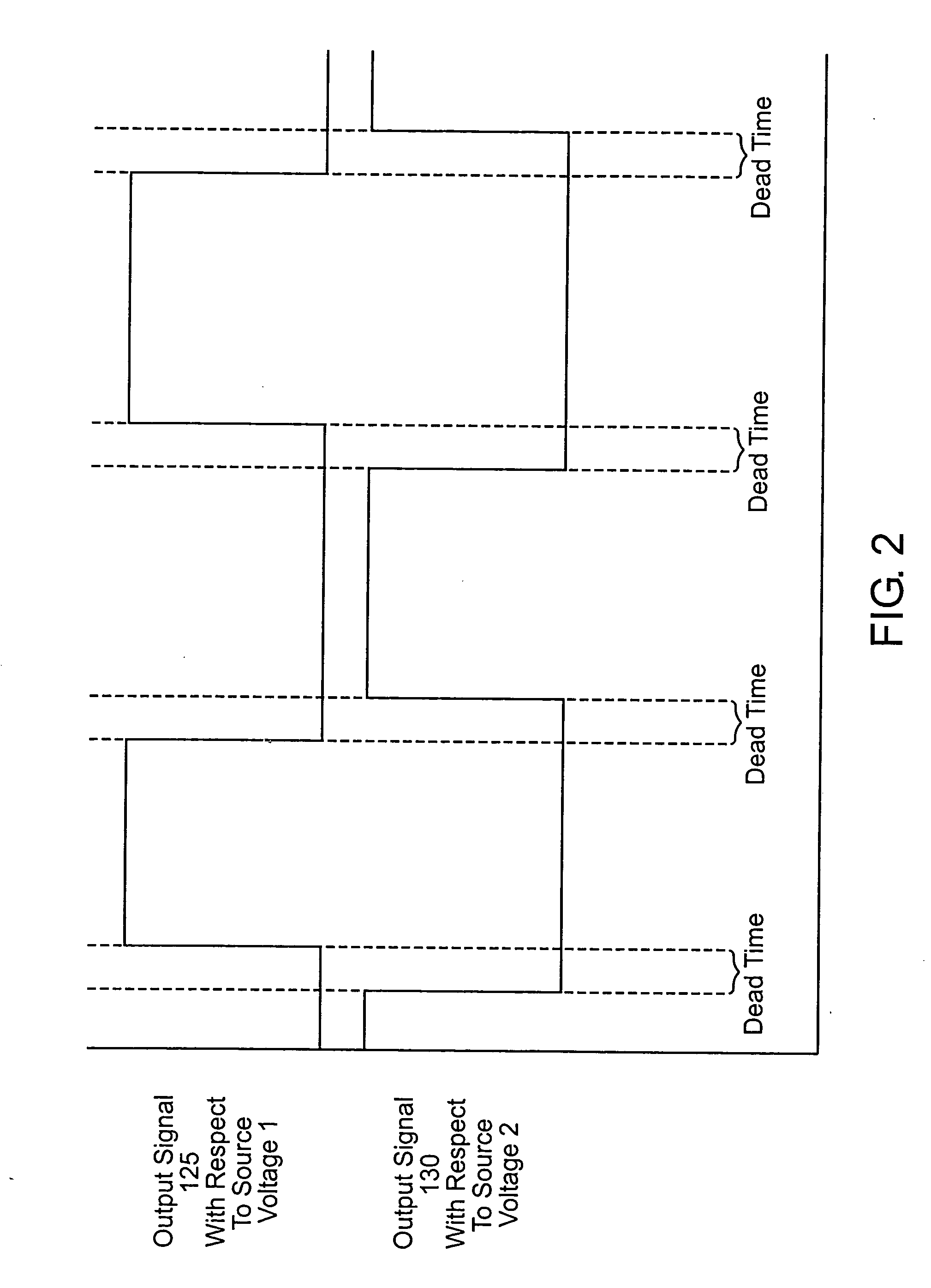
Thus, the ideal “anti-phase” control may not prevent simultaneous conduction of gated switches 115, 120.

Method used


Image

  • Mosgate driver integrated circuit with adaptive dead time
  • Mosgate driver integrated circuit with adaptive dead time
  • Mosgate driver integrated circuit with adaptive dead time

Examples


Embodiment Construction

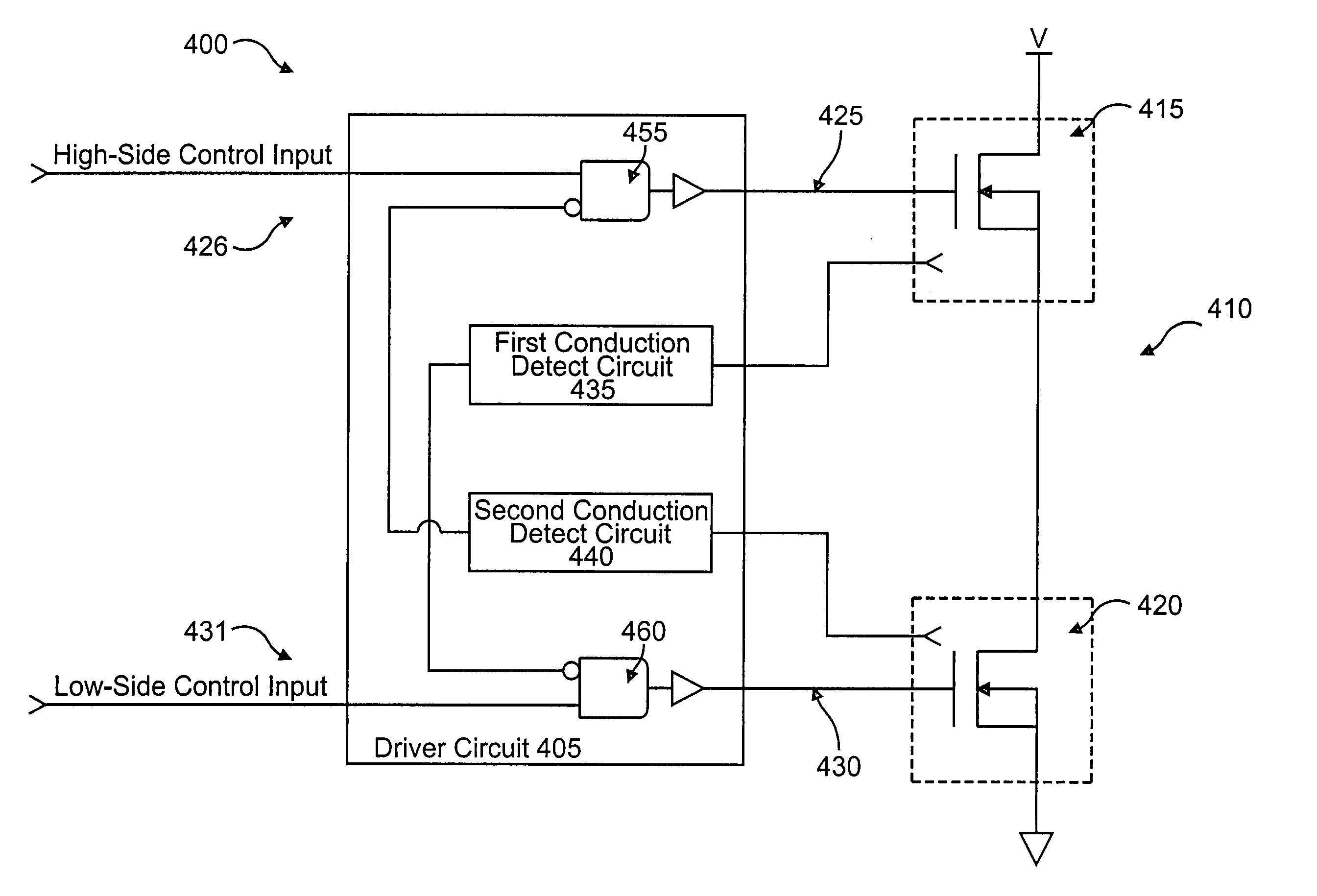
[0016] Referring now to FIG. 4, there is seen an exemplary MOS-gated circuit 400 according to the present invention. MOS-gated circuit 400 includes a bridge leg 410 (or other circuit component) having first and second gated switches 415, 420 electrically coupled to one another in series, as well as a driver circuit 405 for controlling the conduction state of gated switches 415, 420. For this purpose, driver circuit 405 generates respective output signals 425, 430, which are controlled in accordance with high-side and low-side control inputs 426, 431 to control the conduction states of gated switches 415, 420, respectively.

[0017] Although FIG. 4 shows a MOS-gated circuit 400 configured to control the conduction states of two gated switches 415, 420 of bridge leg 410, it should be appreciated that MOS-gated circuit 400 may be employed to control any number of gated switches in any configuration, such as, for example, four gated switches in an H-bridge configuration.

[0018] To prevent...


PUM


Abstract

An IGBT device, comprising a substrate having a conductivity type; a drain electrode arranged on a bottom surface of the substrate; an epitaxial layer arranged on the substrate and having a conductivity type opposite that of the substrate; at least one body diffusion arranged within the epitaxial layer and having a conductivity type the same as that of the substrate; at least one source diffusion arranged within the body diffusion and having a conductivity type the same as that of the epitaxial layer; a gate electrode to control the IGBT device; a source electrode electrically coupled to the body diffusion and the source diffusion; an additional diffusion arranged within the epitaxial layer and having a conductivity type the same as that of the substrate, the additional diffusion forming a collector region of a vertical bipolar arrangement in the IGBT; and a sense electrode electrically coupled to the additional diffusion; wherein the presence of minority carriers in the epitaxial layer may be detected in accordance with a voltage of the sense electrode.

Description

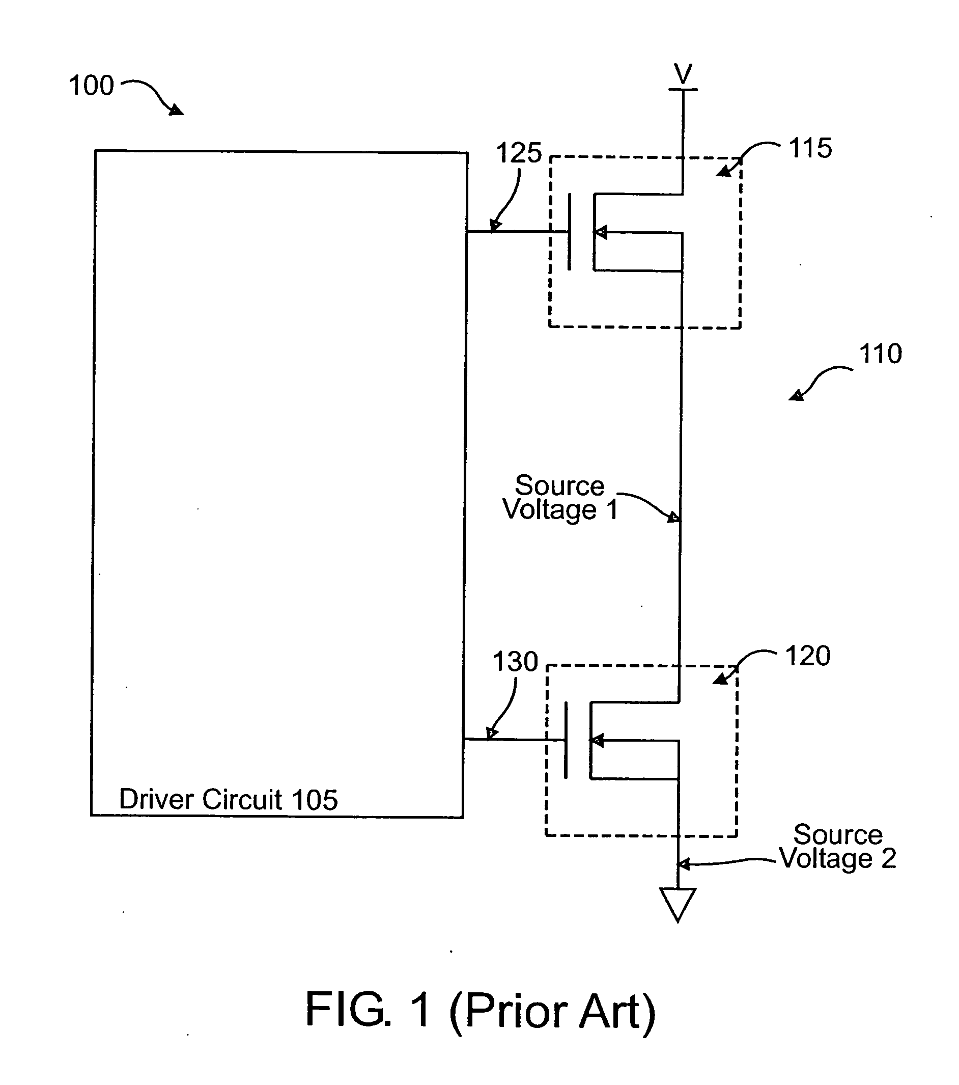
CROSS REFERENCE TO RELATED APPLICATIONS [0001] The present application is a divisional of U.S. patent application Ser. No. 10 / 456,686, filed Jun. 5, 2003 in the name of International Rectifier Corporation and entitled MOSGATE DRIVER INTEGRATED CIRCUIT WITH ADAPTIVE DEAD TIME.FIELD OF THE INVENTION [0002] This invention relates to driver circuits for gated switching devices, for example, a MOSgate driver circuit for driving first and second series connected MOS-gated devices. BACKGROUND OF THE INVENTION [0003] With respect to various applications (e.g., integrated circuit applications), it is known to employ driver circuits for driving at least two gated switches, for example, at least two gated power switches and / or power MOSgated devices (e.g., MOSFETs, IGBTs, GTO Thyristors, etc.). Referring now to FIG. 1, there is seen an exemplary MOS-gated circuit 100 according to the prior art. MOS-gated circuit 100 includes first and second gated switches 115, 120 electrically coupled to one ...

Claims


Application Information

Patent Timeline
Patent Type & Authority Applications(United States)
IPC IPC(8): H01L21/822H01L27/04H01L29/78H02M1/00H02M1/088H02M1/38H03K17/082H03K17/16H03K17/687
CPCH02M1/088H03K17/0822H02M1/38
Inventor NADD, BRUNO
Owner INFINEON TECH AMERICAS CORP
Learn More