Electronic circuit and control method therefor

Inactive Publication Date: 2005-09-15
HITACHI LTD
View PDF11 Cites 19 Cited by
  • Summary
  • Abstract
  • Description
  • Claims
  • Application Information

AI Technical Summary

Benefits of technology

[0015] A first measure to enhance the reception sensitivity is to improve the sensitivity of the RF chip. However, it is considered difficult to further improve the present level according to the present CMOS technology. Under these circumstances, a method is widely executed that improves the reception sensitivity by adding an external RF low noise amplifier (LNA). Theoretically, a communication distance of about 10 m is contemplated implementable if the received signal is amplified up to about 20 dB by adding such an amplifier.
[0020] Therefore, an object of the present invention is to provide a small, long-life, and practical sensor node, which eliminates noise influence as much as possible to enhance more effective reception sensitivity by the amplifier LNA and whose peak current is suppressed to be lower while the standby current is suppressed as much as possible and in which the phenomenon of capacity deterioration of the button battery is reduced.
[0021] Another object of the present invention is to further provide a control method that totally controls a processor chip / RF chip / LNA / sensor in the sensor node to maximally prolong the battery life and thereby enables the standby current and the peak current to be minimized.
[0025] The present invention has a practical communication-distance function and so allows the sensor node having practical operation life to be achieved.

Problems solved by technology

More specifically, a chip capable of performing stable transmission and reception at a distance of several tens meters becomes incommunicable even at a distance of several meters.
Even in this case, however, the radio intensity is deteriorated by as much as 40 dB (=20×log (50 mV / 0.5 mV)), so that deterioration in the communicable distance is unavoidable.
However, it is considered difficult to further improve the present level according to the present CMOS technology.

Method used


Image

  • Electronic circuit and control method therefor
  • Electronic circuit and control method therefor
  • Electronic circuit and control method therefor

Examples


Embodiment Construction

[0047] Embodiments of the present invention will be described hereinafter with reference to the drawings. Note that components denoted by the same reference numeral indicate the same or similar configuration.

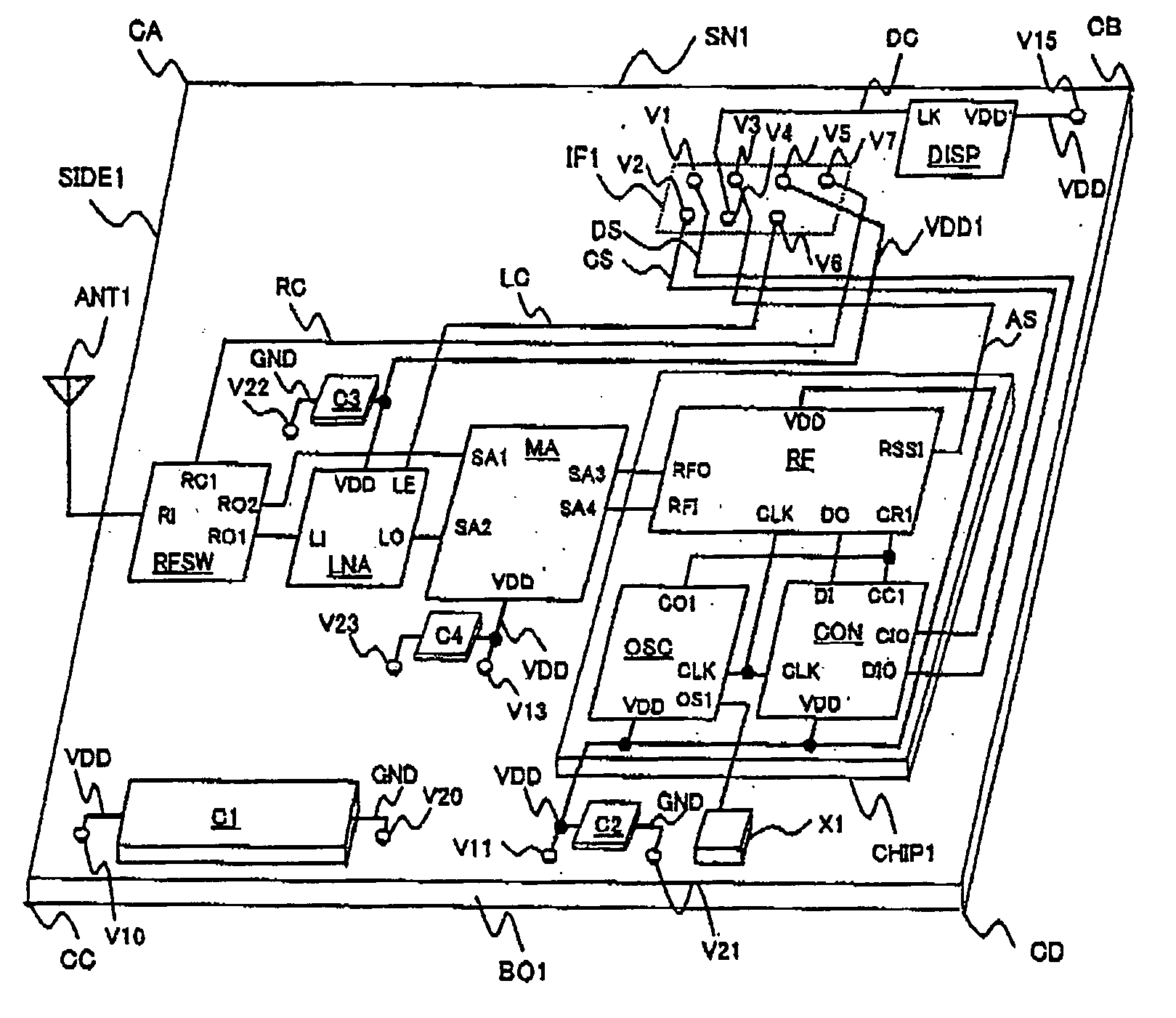
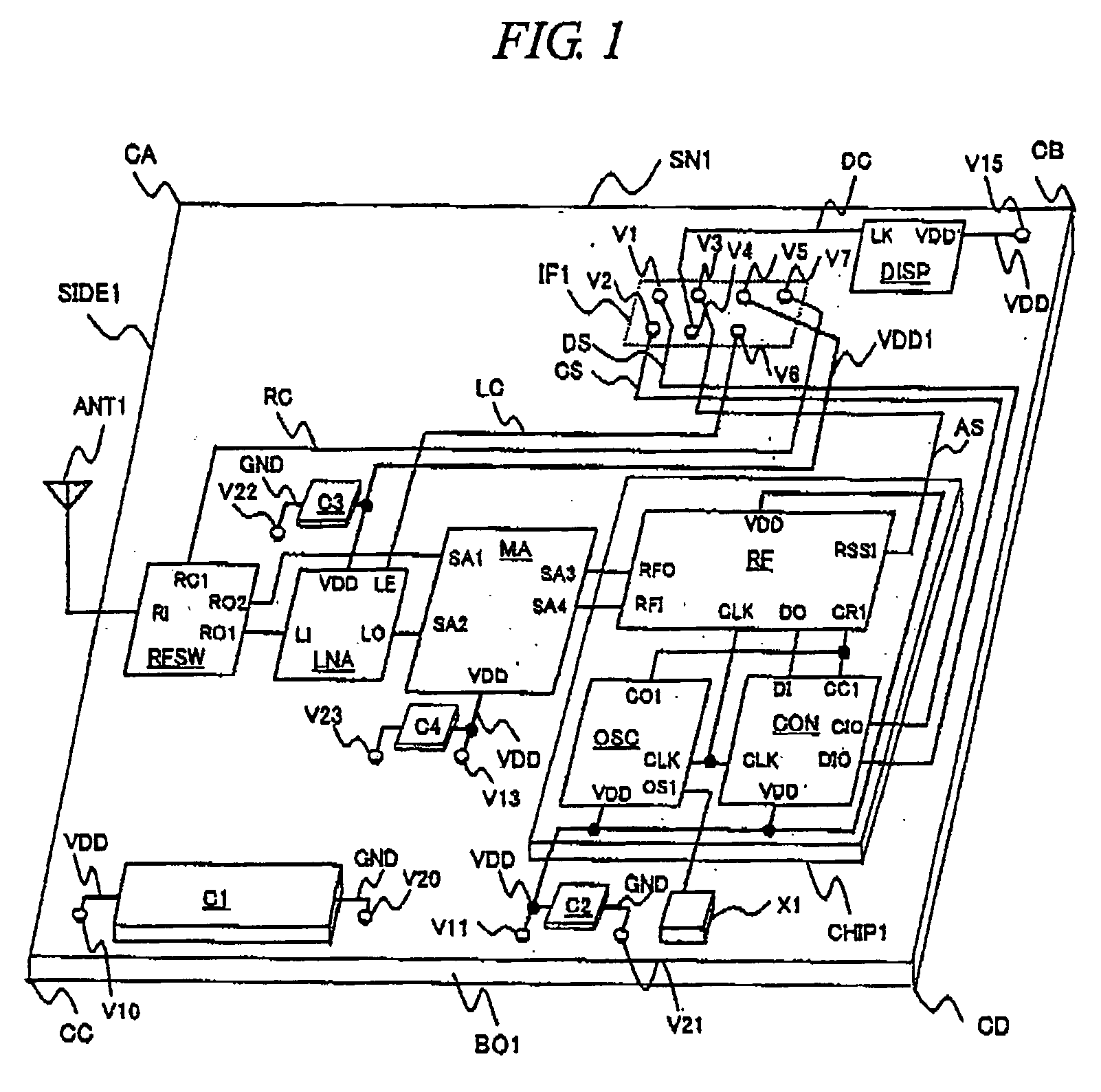
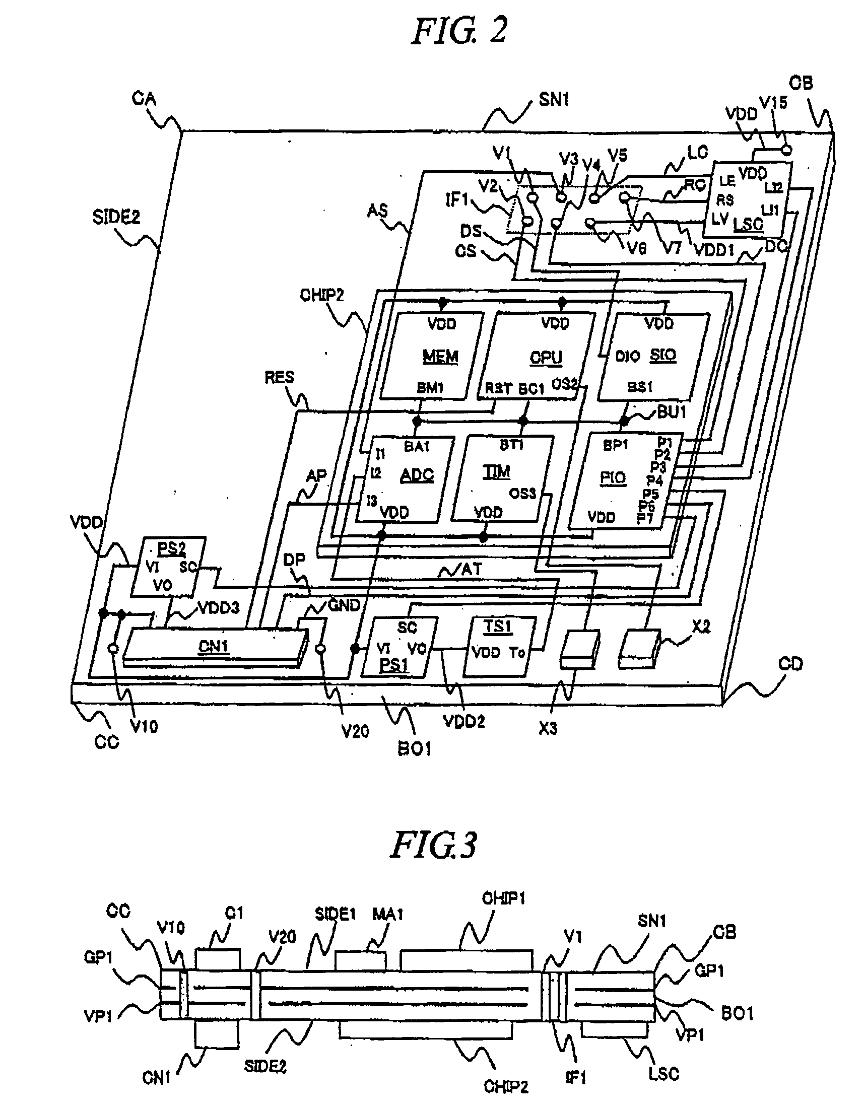
[0048]FIG. 1 shows a state where circuits constituting a sensor node SN1 are mounted on a front side (surface) SIDE1 of a board BO1; and FIG. 2 shows a state where the circuits constituting the sensor node SN1 are mounted on a rear side (surface) SIDE2. Referring to FIG. 1, mounted on the front side SIDE1 of the board BO1 are a high-frequency signal processor chip CHIP1 (hereinafter abbreviated as “RF chip”); a first crystal oscillator X1; a high-frequency switch RFSW; a high-frequency low-noise amplifier LNA; a matching circuit MA; an interface IF1 with the circuits mounted on the rear side SIDE2; a display device DISP; and capacitors C1, C2, C3, and C4. Also, with reference to FIG. 2, the rear side SIDE2 is configured of a processor chip CHIP2; a connector CN1; first and seco...


PUM


Abstract

An electronic circuit, preferable as a sensor node, has a highly sensitive radio function and is capable of performing a low-power-consumption operation. The electronic device has a board; a connector for connecting a sensor; a first signal processor circuit receiving an input of sensor data from the sensor through the connector and forming transmission data; and a second signal processor circuit converting a transmission signal from the first signal processor circuit into a high-frequency signal. The connector and the first signal processor circuit are mounted on a first surface of the board, and the second signal processor circuit is mounted on a second surface of the board.

Description

CROSS-REFERENCE TO RELATED APPLICATION [0001] The present application claims priority from Japanese patent application No. JP 2004-064973 filed on Mar. 9, 2004, the content of which is hereby incorporated by reference into this application. BACKGROUND OF THE INVENTION [0002] The present invention relates to an electronic circuit equipped with a radio communication function. More specifically, the invention relates to a small and low-power-consumption electronic circuit effectively applied to construct a sensor network system. [0003] In recent years, there has been considered a network system (hereinafter abbreviated as “sensor net” for capturing in real time various real-world information into an information-processing device by adding, to a sensor, a small electronic circuit having a radio communication function. For the sensor net, widespread application is considered. For example, there is also considered the application to a medical technology for: always monitoring the pulse et...

Claims


Application Information

Patent Timeline
IPC IPC(8): F24F11/02H04B1/38H04B1/44H05K1/00H05K1/02H05K1/18H05K7/06
CPCH05K1/0218H05K1/0298H05K1/181H05K2203/1572H05K2201/10151H05K2201/10689H05K2201/0723Y02P70/50
Inventor YAMASHITA, SHUNZO
Owner HITACHI LTD
Why Eureka
Try Eureka