Eureka AIR delivers breakthrough ideas for toughest innovation challenges, trusted by R&D personnel around the world.

Semiconductor photodetector device

Inactive Publication Date: 2005-09-01
PANASONIC CORP
View PDF3 Cites 20 Cited by
  • Summary
  • Abstract
  • Description
  • Claims
  • Application Information

AI Technical Summary

Benefits of technology

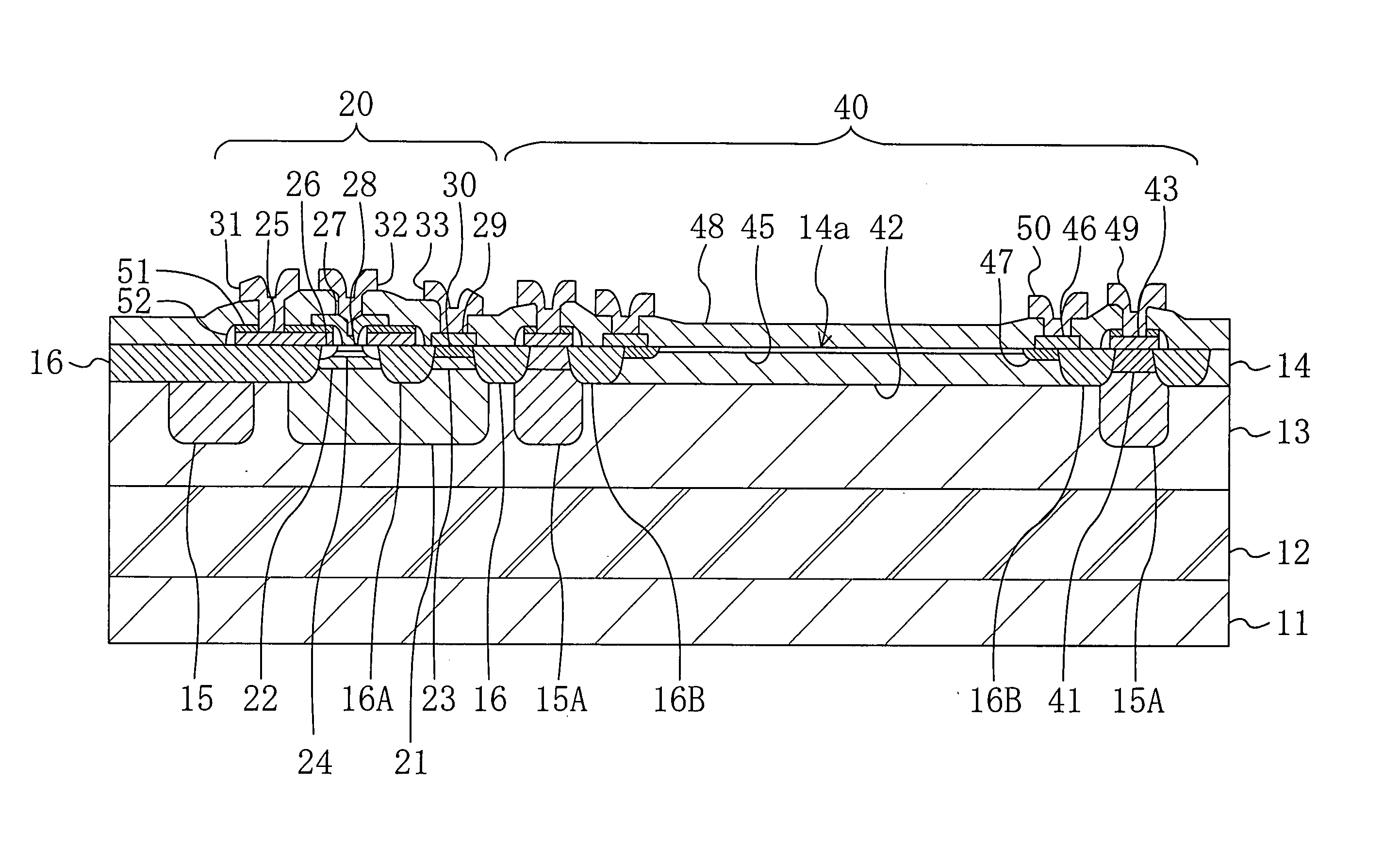
[0039] In the first semiconductor photodetector device, the second region of the first semiconductor layer is used as an active region of a photodetector and, in addition, the second semiconductor layer is used as an active region of a bipolar transistor. This structure includes only one pn junction formed between the third region of the second semiconductor layer and the second region of the first semiconductor layer. Red light and infrared light are mainly received by a depletion layer formed in the second region of the first semiconductor layer. Accordingly, the thickness of the second region is secured so that a sufficient depletion region is formed in a photodetector, thus enhancing light sensitivity. In the second semiconductor layer located in a surface part of the light-receiving face, an internal electric field is generated because of the difference in impurity concentration between the third and forth regions of the same conductivity type. This internal electric field is utilized to obtain photoelectric current from carriers generated from incident light. Accordingly, light is not received only in the depletion layer as in conventional examples, but is received by utilizing the internal electric field. As a result, light sensitivity is higher than those in the conventional examples. In addition, one pn junction is used for light reception, so that parasitic capacitance is reduced and thus high-frequency characteristics of the photodetector are improved.
[0062] In the third semiconductor photodetector device according to the present invention, the impurity concentration of the third region of the second conductivity type is set equal to or higher than that of the second region of the first conductivity type, so that a depletion layer formed in the second region is extended to the third region without suppressing extension thereof. Accordingly, capacitance is reduced as compared to the conventional examples, and frequency characteristics are improved. In addition, in the second semiconductor layer of the second conductivity type having the third and fourth regions and constituting the light-receiving region of a photodetector, the fourth region is formed in the third region and has an impurity concentration higher than that of the third region, so that the frat portion (represented by the symbol d in FIG. 11B) of the potential formed in the third region is shortened, and thus frequency characteristics in the third region are improved. Accordingly, in the third semiconductor photodetector device according to the present invention, the structure including the third region and the forth region formed in the third region allows the thickness of the third region to be increased. As a result, a vertical pnp-transistor (VPNP-Tr) is formed without deterioration of characteristics of the photodetector.

Problems solved by technology

This causes deterioration of high-frequency characteristics of the photodetector.
As a result, there arises a problem in which high-frequency characteristics of the bipolar transistor 20 are impaired.
However, the influence of the junction capacitances of the pn junctions prevents sufficient improvement of the high-frequency characteristics even in the second conventional example.
Accordingly, the pn junction capacitances due to the isolation are added to these elements, so that a cause of deterioration of high-frequency characteristics arises.
Accordingly, in the structures of photodetectors of the first and second conventional examples, light is received at a position at which the amount of absorbed blue light is small, so that sufficient light sensitivity to blue light is unlikely to be obtained.
However, in the OEIC devices of the first and second conventional examples, if the thickness of the anode region 242 is reduced, a sufficient depletion layer is not formed in the n-type semiconductor layer 202, so that it is difficult to enhance light sensitivity to light with a short wavelength.
However, the third conventional example has a problem in which the n-type semiconductor region 304 has a small thickness of 1 μm or less, so that a vertical pnp-transistor (VPNP-Tr) exhibiting high-speed response is not formed.
However, this enlarges a peripheral region of the photodetector part 100, and a problem in which the chip area cannot be reduced arises.

Method used


Image

  • Semiconductor photodetector device
  • Semiconductor photodetector device
  • Semiconductor photodetector device

Examples


embodiment 1

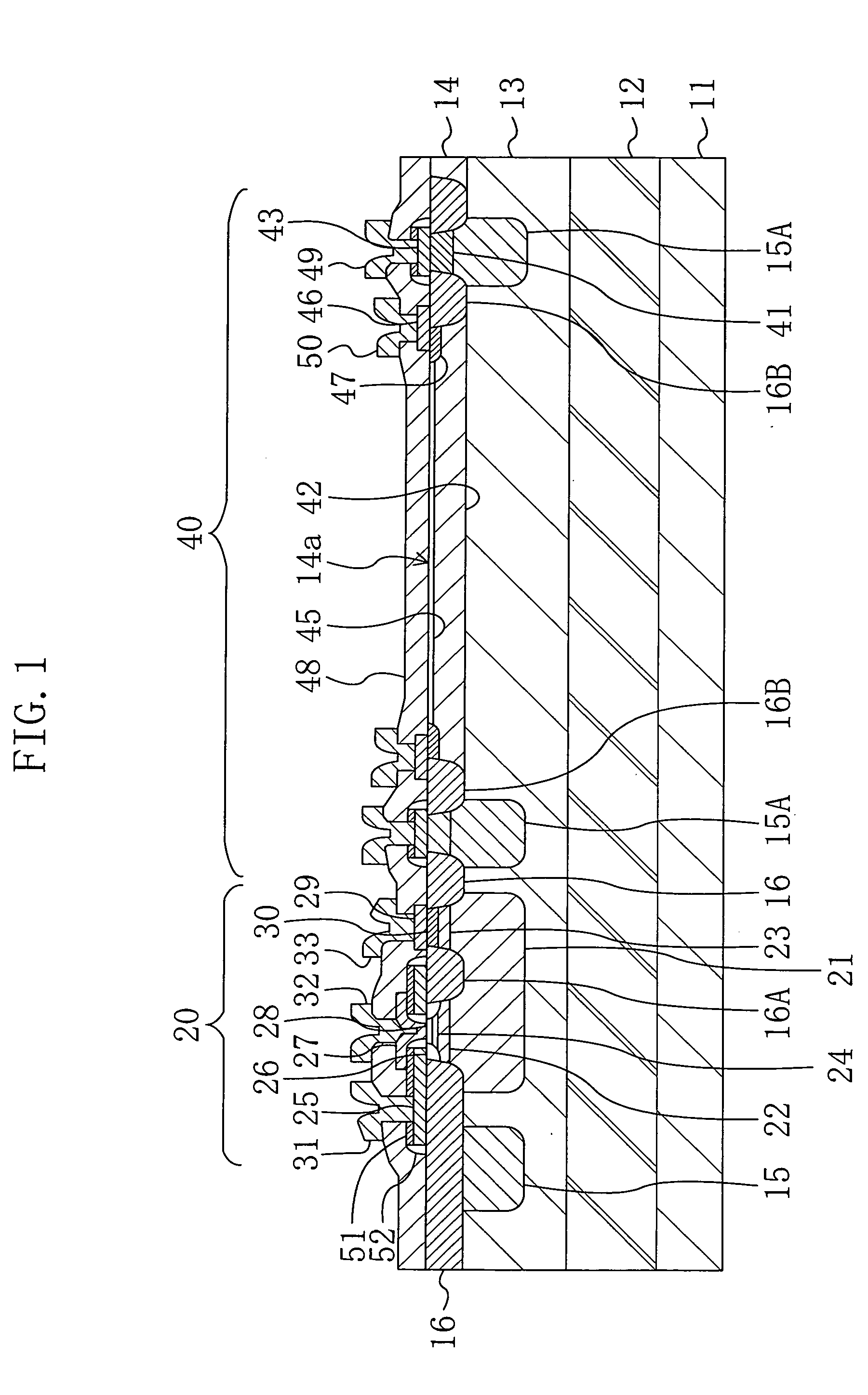
[0082] A semiconductor photodetector device according to a first embodiment of the present invention will be described with reference to drawings.

[0083]FIG. 1 shows a cross-sectional structure of the semiconductor photodetector device of the first embodiment. As shown in FIG. 1, a first p-type semiconductor layer (a first region of a first semiconductor layer) 12 containing a p-type impurity at a high concentration, a second p-type semiconductor layer (a second region of the first semiconductor layer) 13 containing an n-type impurity at a concentration lower than that of the first p-type semiconductor layer 12 and an n-type semiconductor layer (a second semiconductor layer) 14 containing an n-type impurity at a concentration higher than that of the second p-type semiconductor layer 13 are formed in this order over a substrate 11 made of p-type silicon. Over the substrate 11, a region where an npn-bipolar transistor 20 is formed and a region where a photodiode 40 of a cathode common...

modified example 1 of embodiment 1

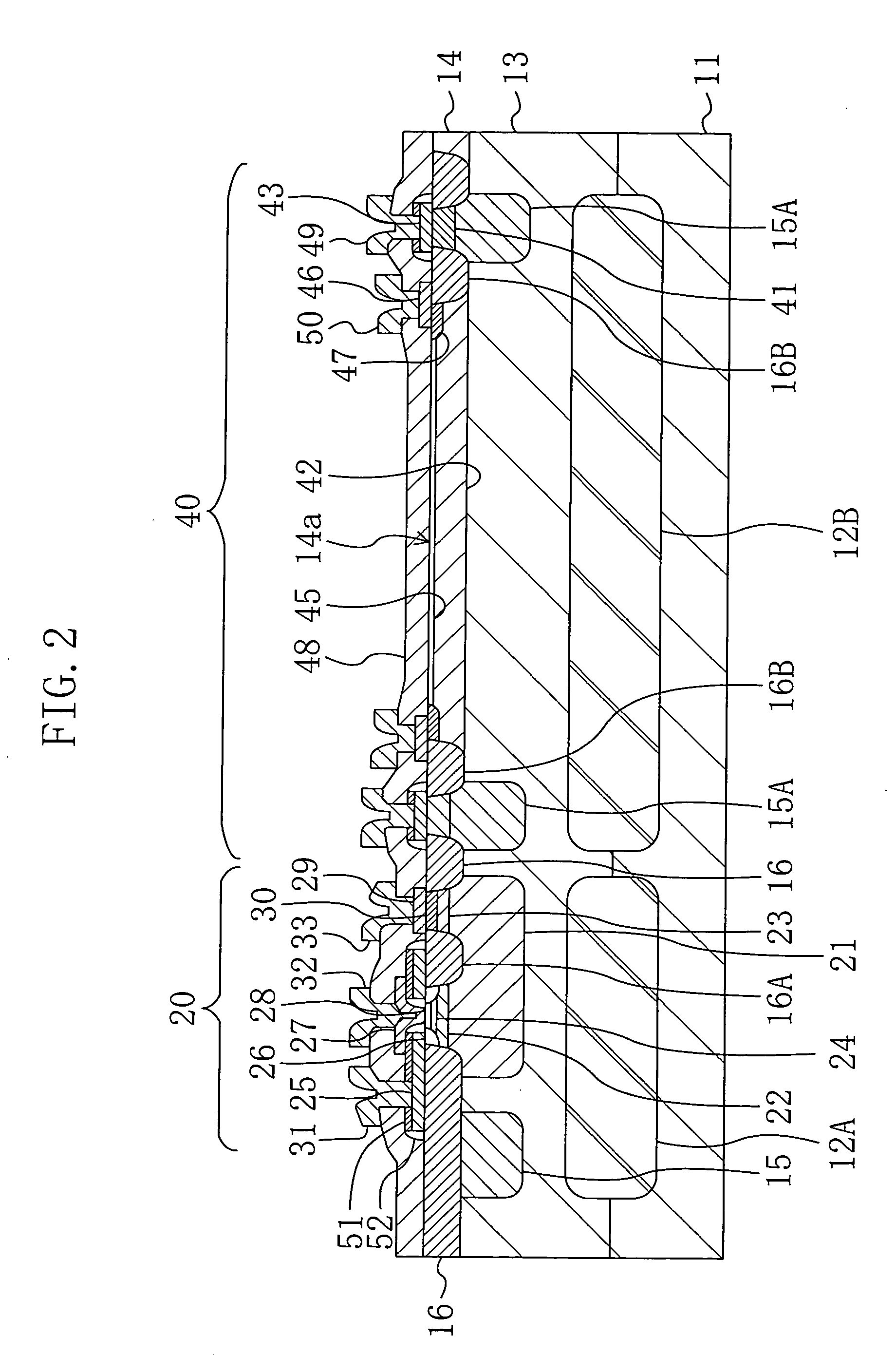
[0100]FIG. 2 shows a cross-sectional structure of a semiconductor photodetector device according to a first modified example of the first embodiment. In FIG. 2, each member already shown in FIG. 1 is identified by the same reference numeral and the description thereof will be omitted herein.

[0101] As shown in FIG. 2, in the semiconductor photodetector device of the first modified example, instead of the first p-type semiconductor layer 12 shown in FIG. 1, p-type buried regions 12A and 12B are selectively formed in a transistor region where a bipolar transistor 20 is formed and a region where a photodiode 40 is formed, respectively.

[0102] In the OEIC device, the bipolar transistor 20 has a circuit configuration in which amplification is performed using a light signal received by the photodiode 40 as an input signal. Accordingly, the amplified signal with a large amplitude is superimposed onto a collector-lower-part extraction region 21, so that parasitic capacitance between the col...

modified example 2 of embodiment 1

[0105]FIG. 3 shows a cross-sectional structure of a semiconductor photodetector device according to a second modified example of the first embodiment. In FIG. 3, each member already shown in FIG. 1 is identified by the same reference numeral and the description thereof will be omitted herein.

[0106] As shown in FIG. 3, the semiconductor photodetector device of the second modified example is different from the device shown in FIG. 1 in that a bipolar transistor 20 and a photodiode 40 are placed at a given distance from each other and an isolation insulating film 16 has a large width. In this configuration of the second modified example, inductive coupling between the bipolar transistor 20 and the photodiode 40 is reduced, so that it is possible to suppress entering of an alternating current signal amplified by the bipolar transistor 20 into the photodiode. As a result, reduction of the S / N ratio resulting from entering of the signal is also suppressed. The given distance is a clearan...


PUM


Abstract

A semiconductor photodetector device includes: a first semiconductor layer of a first conductivity type; and a second semiconductor layer of a second conductivity type formed on the first semiconductor layer and having a light-receiving region. The first semiconductor layer includes a first region containing an impurity of the first conductivity type at a high concentration and a second region formed on the first region and containing an impurity of the first conductivity type at a concentration lower than that of the first region. The second semiconductor layer includes a third region containing an impurity of the second conductivity type at a concentration higher than that of the second region and a fourth region formed on the third region and containing an impurity of the second conductivity type at a concentration higher than that of the third region.

Description

CROSS-REFERENCE TO RELATED APPLICATION [0001] The disclosures of Japanese Patent Applications Nos. 2004-56681 and 2004-309537 filed on Mar. 1, 2004 and Oct. 25, 2004, respectively, including claims, specifications, drawings and claims are incorporated herein by reference in their entirety. BACKGROUND OF THE INVENTION [0002] The present invention relates to semiconductor photodetector devices, and particularly to a semiconductor photodetector device in which a photodetector and a logic element are formed on the same substrate. [0003] Opto-electronic integrated circuit (OEIC) devices in each of which a photodetector such as a photodiode converting a light signal into an electric signal and a logic element such as a transistor and a capacitor constituting a peripheral circuit are formed on a substrate are known to date as semiconductor photodetector devices, and have been used as optical pickup devices for compact discs (CDs) or digital versatile discs (DVDs), for example. [0004] Herei...

Claims


Application Information

Patent Timeline
IPC IPC(8): H01L27/144H01L27/15H01L31/0288H01L31/103
CPCH01L27/1443Y02E10/50H01L31/103H01L31/0288
Inventor YASUKAWA, HISATADAITO, RYOUICHIIWAI, TAKAKITANIGUCHI, MASAKIJIN, YASUSHI
Owner PANASONIC CORP
Why Eureka
Eureka Blog
Learn More