
Laser processing method and laser processing apparatus

a laser processing and laser processing technology, applied in the direction of conveyors, manufacturing tools, instruments, etc., can solve the problems of laser deviation, unnecessary fractures, laser may occur, etc., and achieve the effect of no unnecessary fractures on the surfa

Inactive Publication Date: 2005-08-18
HAMAMATSU PHOTONICS KK
View PDF91 Cites 127 Cited by
  • Summary
  • Abstract
  • Description
  • Claims
  • Application Information

AI Technical Summary

Benefits of technology

The present invention provides laser processing methods and apparatus that do not generate unnecessary fractures or melt in the surface of an object being processed. These methods use a laser with a light-converging point to create a modified region within the object along a line along which it is intended to be cut. The modified region is formed by inducing thermal distortion and optical damage through multiphoton absorption. The laser processing methods and apparatus of this invention allow for precise and safe cutting without damaging the surface of the object being processed.

Problems solved by technology

However, this method also melts surroundings of the region to become the cutting part in the surface of the object to be cut.
When the thermal shock generated in the object to be processed is large in the cutting methods of the above-mentioned publications, unnecessary fractures such as those deviating from lines along which the object is intended to be cut or those extending to a part not irradiated with laser may occur.
Therefore, these cutting methods cannot achieve precision cutting.
When the object to be processed is a semiconductor wafer, a glass substrate formed with a liquid crystal display device, or a glass substrate formed with an electrode pattern in particular, semiconductor chips, liquid crystal display devices, or electrode patterns may be damaged due to the unnecessary fractures.
Also, average input energy is so high in these cutting methods that the thermal damage imparted to the semiconductor chip and the like is large.

Method used


Image

  • Laser processing method and laser processing apparatus
  • Laser processing method and laser processing apparatus
  • Laser processing method and laser processing apparatus

Examples


first embodiment

[0281] [First Embodiment]

[0282] The laser processing method in accordance with a first embodiment of the present invention will be explained. FIG. 14 is a schematic diagram of a laser processing apparatus 100 usable in this method. The laser processing apparatus 100 comprises a laser light source 101 for generating laser light L; a laser light source controller 102 for controlling the laser light source 101 so as to regulate the output and pulse width of laser light L and the like; a dichroic mirror 103, arranged so as to change the orientation of the optical axis of laser light L by 90°, having a function of reflecting the laser light L; a light-converging lens 105 for converging the laser light L reflected by the dichroic mirror 103; a mounting table 107 for mounting an object to be processed 1 irradiated with the laser light L converged by the light-converging lens 105; an X-axis stage 109 for moving the mounting table 107 in the X-axis direction; a Y-axis stage 111 for moving th...

second embodiment

[0303] [Second Embodiment]

[0304] A second embodiment of the present invention will now be explained. This embodiment is directed to a cutting method and cutting apparatus for a light-transmitting material. The light-transmitting material is an embodiment of the objects to be processed. In this embodiment, a piezoelectric device wafer (substrate) having a thickness of about 400 pm made of LiTaO3 is used as a light-transmitting material.

[0305] The cutting apparatus in accordance with the second embodiment is constituted by the laser processing apparatus 100 shown in FIG. 14 and the apparatus shown in FIGS. 19 and 20. The apparatus shown in FIGS. 19 and 20 will be explained. The piezoelectric device wafer 31 is held by a wafer sheet (film) 33 acting as holding means. In the wafer sheet 33, the face on the side holding the piezoelectric device wafer 31 is made of an adhesive resin tape or the like, and has an elasticity. The wafer sheet 33 is set on a mounting table 107 while being hel...

third embodiment

[0357] [Third Embodiment]

[0358] A third embodiment of the present invention will be explained. In the third embodiment and a fourth embodiment which will be explained later, an object to be processed is irradiated with laser light such that the direction of linear polarization of linearly polarized laser light extends along a line along which the object is intended to be cut in the object to be processed, whereby a modified region is formed in the object to be processed. As a consequence, in the modified spot formed with a single pulse of shot (i.e., a single pulse of laser irradiation), the size in the direction extending along the line along which the object is intended to be cut can be made relatively large when the laser light is pulse laser light. The inventor has confirmed it by an experiment. Conditions for the experiment are as follows: [0359] (A) Object to be processed: Pyrex glass wafer (having a thickness of 700 μm and an outer diameter of 4 inches) [0360] (B) Laser [0361...


PUM

PropertyMeasurementUnit
thicknessaaaaaaaaaa
Moving speedaaaaaaaaaa
thicknessaaaaaaaaaa

Abstract

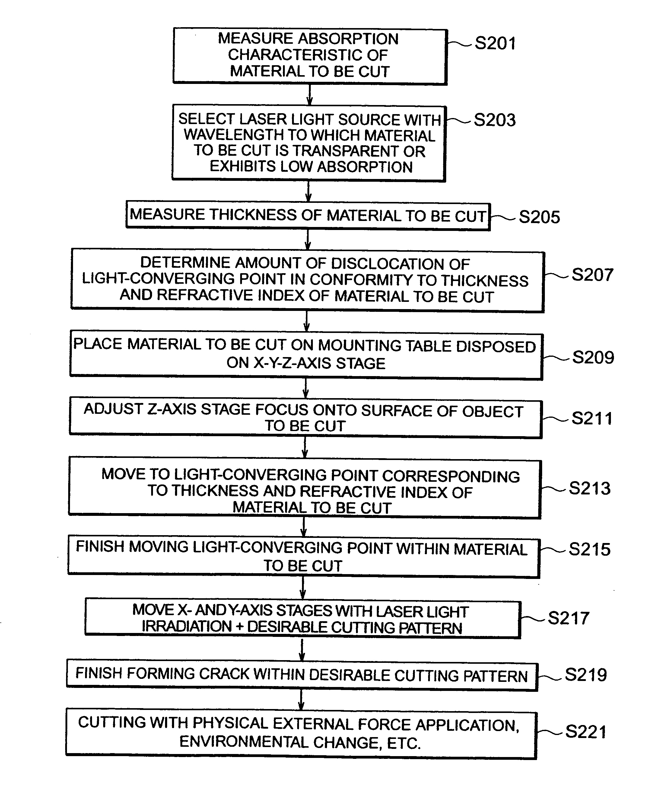
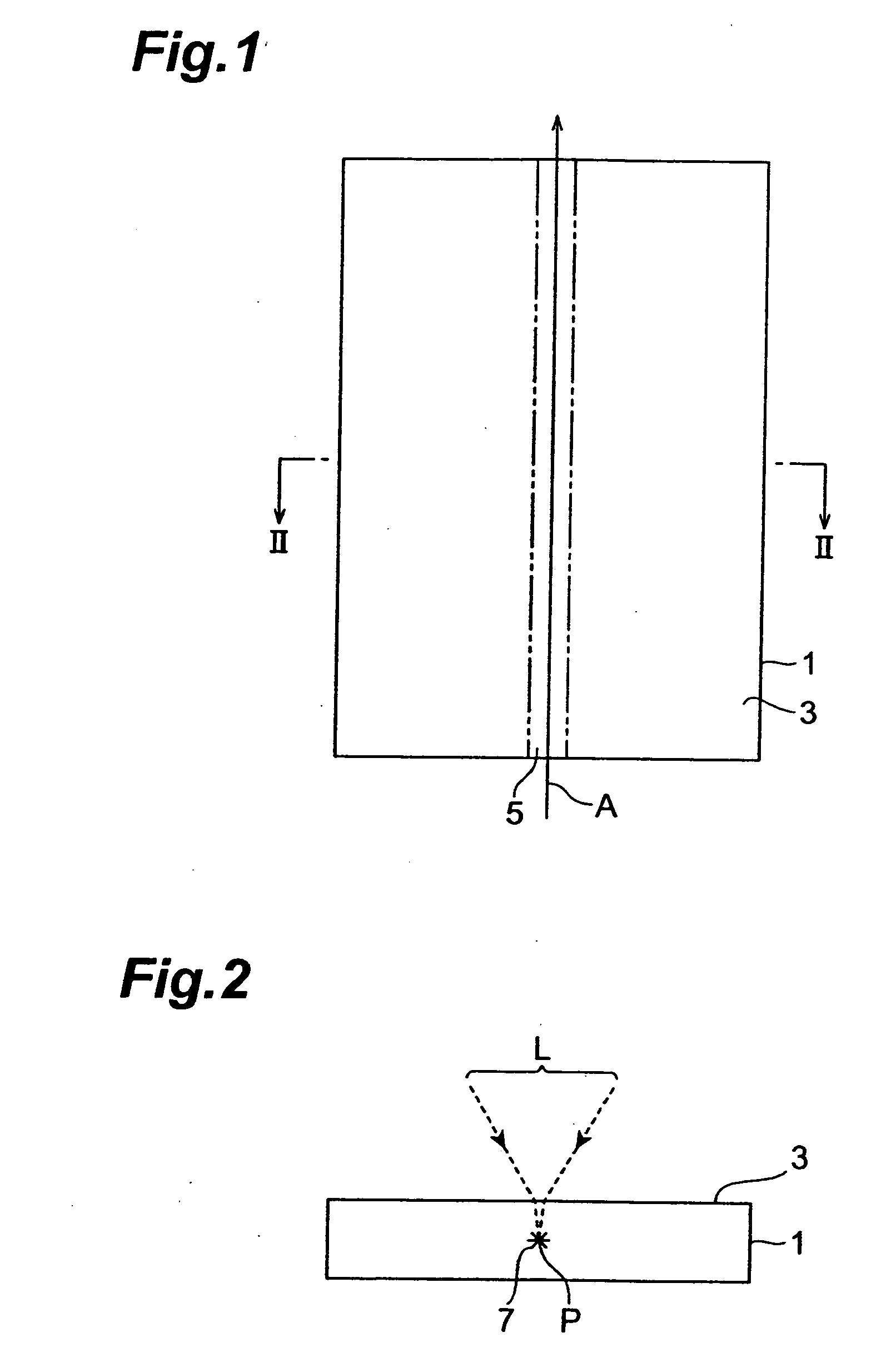
A laser beam machining method and a laser beam machining device capable of cutting a work without producing a fusing and a cracking out of a predetermined cutting line on the surface of the work, wherein a pulse laser beam is radiated on the predetermined cut line on the surface of the work under the conditions causing a multiple photon absorption and with a condensed point aligned to the inside of the work, and a modified area is formed inside the work along the predetermined determined cut line by moving the condensed point along the predetermined cut line, whereby the work can be cut with a rather small force by cracking the work along the predetermined cut line starting from the modified area and, because the pulse laser beam radiated is not almost absorbed onto the surface of the work, the surface is not fused even if the modified area is formed.

Description

CROSS-REFERENCE TO RELATED APPLICATION [0001] This application is a continuing application of PCT Application No. PCT / JP01 / 07954 filed on Sep. 13, 2001, designating U.S.A. and now pending.BACKGROUND OF THE INVENTION [0002] 1. Field of the Invention [0003] The present invention relates to laser processing methods and laser processing apparatus used for cutting objects to be processed such as semiconductor material substrates, piezoelectric material substrates, and glass substrates. [0004] 2. Related Background Art [0005] One of laser applications is cutting. A optical cutting process effected by laser is as follows: For embodiment, a part to be cut in an object to be processed such as a semiconductor wafer or glass substrate is irradiated with laser light having a wavelength absorbed by the object, so that melting upon heating proceeds due to the laser light absorption from the surface to rear face of the object to be processed at the part to be cut, whereby the object to be processe...

Claims


Application Information

Patent Timeline
Patent Type & Authority Applications(United States)
IPC IPC(8): B23K26/073B23K26/38B23K26/40B23K101/40B28D5/00C03B33/023C03B33/08C03B33/09C03B33/10C03C23/00G02F1/1368H01L21/301
CPCB23K26/0057Y10T29/49144B23K26/032B23K26/034B23K26/046B23K26/0635B23K26/0656B23K26/073B23K26/0853B23K26/367B23K26/4075B23K2201/40B28D5/0011B65G2249/04C03B33/023C03B33/082C03B33/102C03C23/0025G02F1/1368B23K26/03B23K26/0624B23K26/066B23K26/364B23K26/53B23K2103/50B23K26/40C03B33/0222C03B33/091B23K26/38B23K26/04B23K26/70B23K26/702B23K2101/40B23K26/16Y02P40/57H01L21/6836H01L2221/68327B23K20/023B23K20/16B23K20/233B23K20/26Y10T83/0341H01L21/78B23K26/08B23K26/36
Inventor FUKUYO, FUMITSUGUFUKUMITSU, KENSHIUCHIYAMA, NAOKIWAKUDA, TOSHIMITSUATSUMI, KAZUHIROMURAMATSU, KENICHI
Owner HAMAMATSU PHOTONICS KK
Learn More