
Semiconductor wafer, apparatus and process for producing the semiconductor wafer

Inactive Publication Date: 2005-08-11
SILTRONIC AG
View PDF11 Cites 54 Cited by
  • Summary
  • Abstract
  • Description
  • Claims
  • Application Information

AI Technical Summary

Benefits of technology

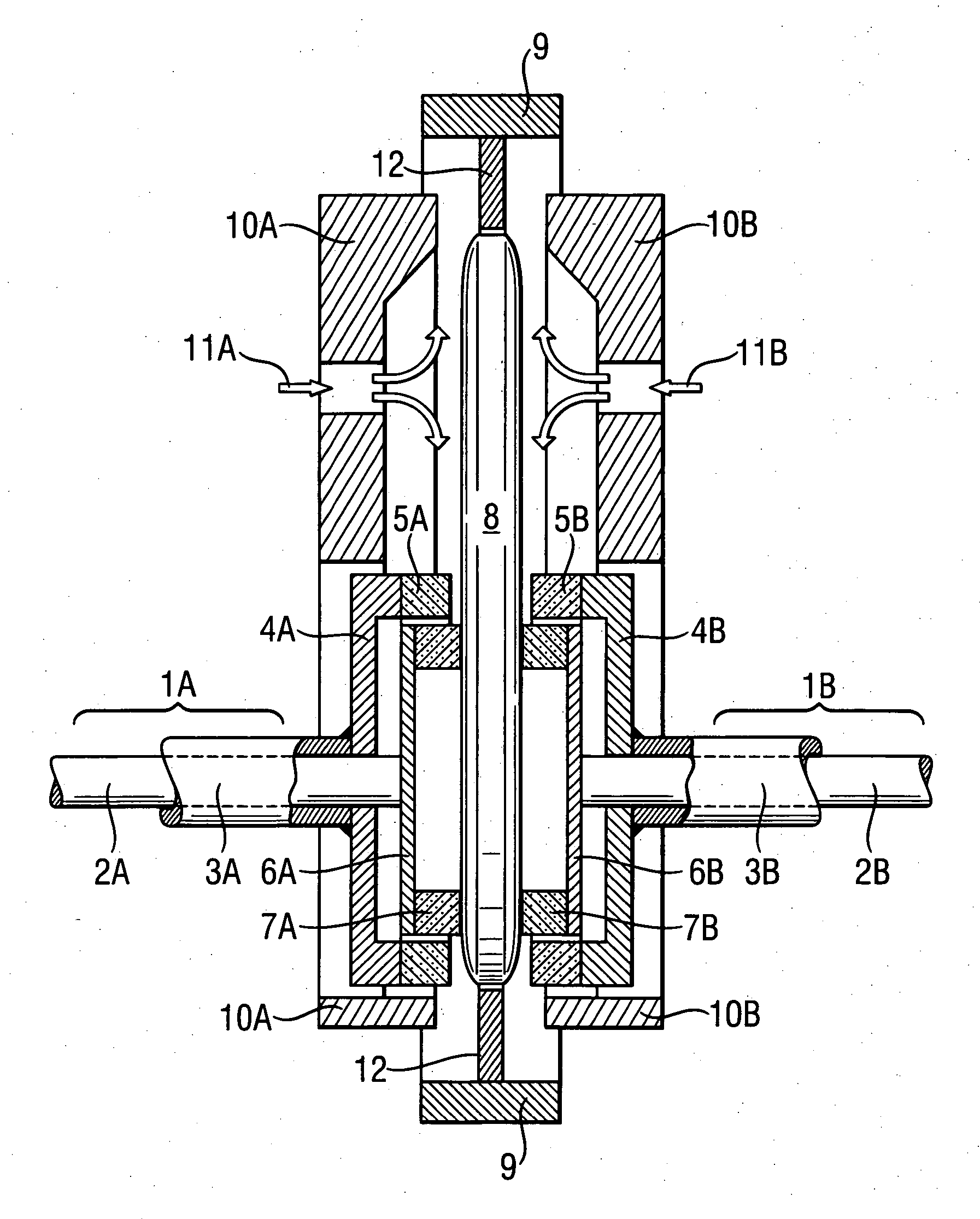
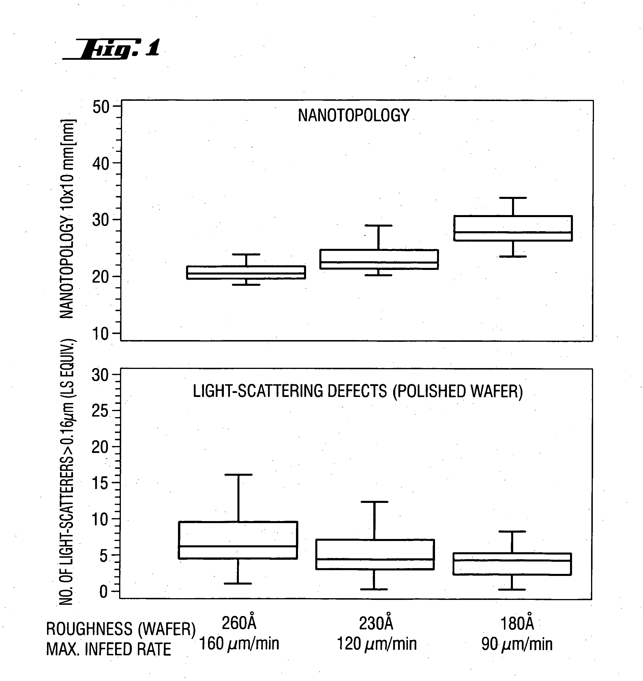
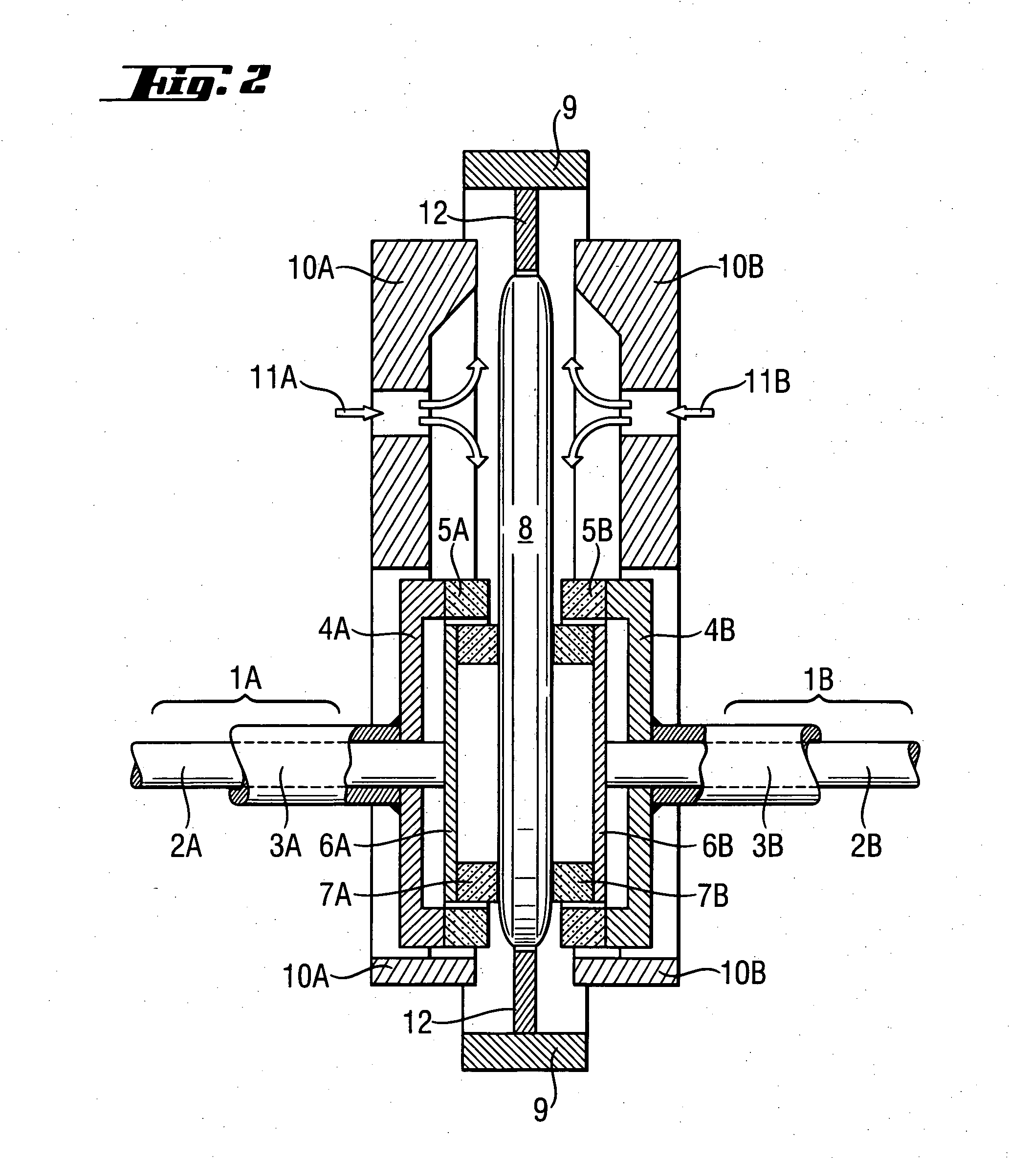
[0024] An object of the present invention is in particular the economic production of an especially flat semiconductor wafer with good nanotopology and a low-damage finish following mechanical machining, which allows a reduction in any removal of material in subsequent process steps which may be necessary. These and other objects are achieved by a process for producing a semiconductor wafer, comprising double-side grinding of the semiconductor wafer, in which the semiconductor wafer is simultaneously ground, on both sides using a grinding tool, firstly by rough-grinding and then by finish-grinding, wherein the semiconductor wafer, between rough-grinding and finish-grinding, remains clamped in a grinding machine, and the grinding tool continues to apply a substantially constant load during the transition from rough-grinding to finish-grinding.

Problems solved by technology

However, this multi-stage process sequence is complex, relatively inflexible, and overall requires very large amounts of material to be removed on account of repeated grinding operations.
In particular, however, the SSG largely destroys the advantages of the preceding DDG.
This process sequence is likewise complex, material-intensive, susceptible to faults, and expensive.

Method used


Image

  • Semiconductor wafer, apparatus and process for producing the semiconductor wafer
  • Semiconductor wafer, apparatus and process for producing the semiconductor wafer
  • Semiconductor wafer, apparatus and process for producing the semiconductor wafer

Examples


application examples

[0052] The following process parameters are among the preferred examples for an application of the DDDG process according to the invention:

[0053] In the case of rough-grinding, these parameters are as follows: a grinding wheel which is held by the inner or outer sub-spindle, has a grain size of 4-50 μm with diamond as the abrasive, ceramically or metallically bonded; grinding removal of 2×20 μm to 2×60 μm at a spindle rotational speed of 1000-12,000 rpm; a spindle infeed rate of 15-300 μm / min (based on both spindles); a semiconductor wafer rotational speed of 5-100 rpm; and cooling lubrication using 0.1-5 l / min of water. The result is a semiconductor wafer with rough-ground side faces having a roughness of 250-3000 Å RMS (using a profilometer with a 1-80 μm filter) and a total thickness variation TTV of 0.7-3 μm in the case of a process with coaxially arranged double spindles during rough-grinding.

[0054] In the case of finishing-grinding, the preferred parameters are: a grinding w...


PUM

PropertyMeasurementUnit
Lengthaaaaaaaaaa
Lengthaaaaaaaaaa
Lengthaaaaaaaaaa

Abstract

The invention relates to a process for producing a semiconductor wafer by double-side grinding of the semiconductor wafer, in which the semiconductor wafer is simultaneously ground on both sides, first by rough-grinding and then by finish-grinding, using a grinding tool. The semiconductor wafer, between the rough-grinding and the finish-grinding, remains positioned in the grinding machine, and the grinding tool continues to apply a substantially constant load during the transition from rough-grinding to finish-grinding. The invention also relates to an apparatus for carrying out the process and to a semiconductor wafer having a local flatness value on a front surface of less than 16 nm in a measurement window of 2 mm×2 mm area and of less than 40 nm in a measurement window of 10 mm×10 mm area.

Description

BACKGROUND OF THE INVENTION [0001] 1. Field of the Invention [0002] The present invention relates to a process for producing an especially planar semiconductor wafer with good nanotopology and a low-damage finish after machining, to a semiconductor wafer of this type, and to an apparatus for the double-side grinding of flat workpieces.[0003] 2. Background Art [0004] Electronics, microelectronics and (micro)electromechanics require starting materials (substrates) with extremely high demands imposed on global and local flatness, thickness distribution, single surface referenced local flatness (nanotopology), roughness, and cleanliness. Depending on the intended use, the substrates used are wafers made from metals, insulators, or semiconductor material, in particular, compound semiconductors such as gallium arsenide, and primarily, elemental semiconductors such as silicon and sometimes germanium. Furthermore, the term semiconductor wafers is also to be understood as meaning substrates ...

Claims


Application Information

Patent Timeline
IPC IPC(8): B24B7/17B24B7/04B24B7/22B24D7/14H01L21/302H01L21/304
CPCB24B7/17H01L21/02013B24D7/14B24B7/228H01L21/304
Inventor PIETSCH, GEORGKERSTAN, MICHAELBLAHA, WERNER
Owner SILTRONIC AG
Learn More