
Non-volatile memory cell comprising a dielectric layer and a phase change material in series

a technology of phase change material and memory cell, which is applied in the direction of digital storage, transistors, instruments, etc., can solve the problems of restricting the usefulness of this approach

Inactive Publication Date: 2005-07-21
SANDISK TECH LLC
View PDF13 Cites 238 Cited by
  • Summary
  • Abstract
  • Description
  • Claims
  • Application Information

AI Technical Summary

Problems solved by technology

The limits of photolithography, however, restrict the usefulness of this approach.

Method used


Image

  • Non-volatile memory cell comprising a dielectric layer and a phase change material in series
  • Non-volatile memory cell comprising a dielectric layer and a phase change material in series
  • Non-volatile memory cell comprising a dielectric layer and a phase change material in series

Examples


Embodiment Construction

[0025] While all materials can change phase, in this discussion the term “phase change material” will be used to describe a material that changes relatively easily from one stable state to another. The phase change is typically from an amorphous state to a crystalline state (or vice versa), but may be an intermediate change, such as from a less-ordered to a more ordered crystalline state, or vice versa. Chalcogenides are well-known phase change materials.

[0026] It is known to use phase change materials, such as chalcogenides, in a nonvolatile memory cell, in which a high-resistance, amorphous state represents one memory state while a low-resistance, crystalline state represents the other memory state, where memory states correspond to a value of 1 or 0. (If intermediate stable states are achieved, more than two memory states can exist for each cell; for simplicity, the examples in this discussion will describe only two memory states.) Chalcogenides are particularly useful examples ...


PUM


Abstract

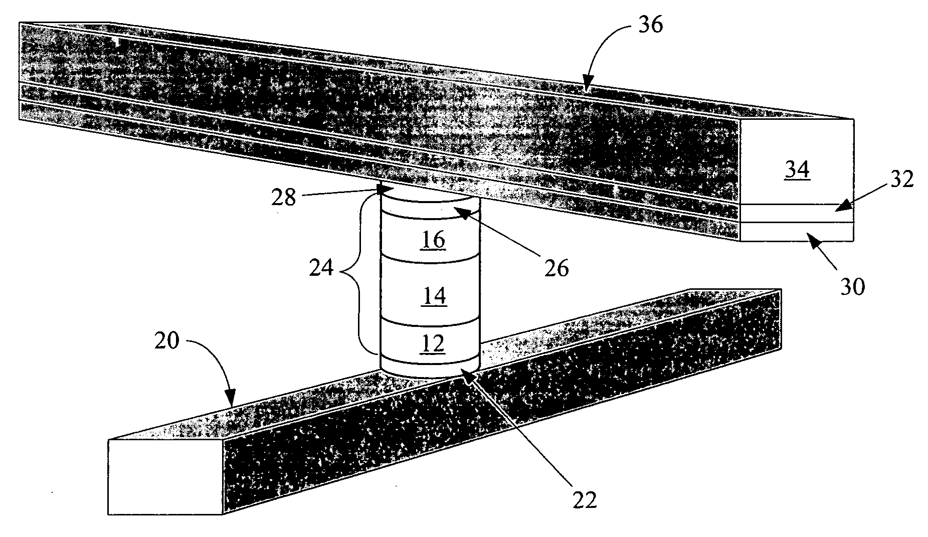
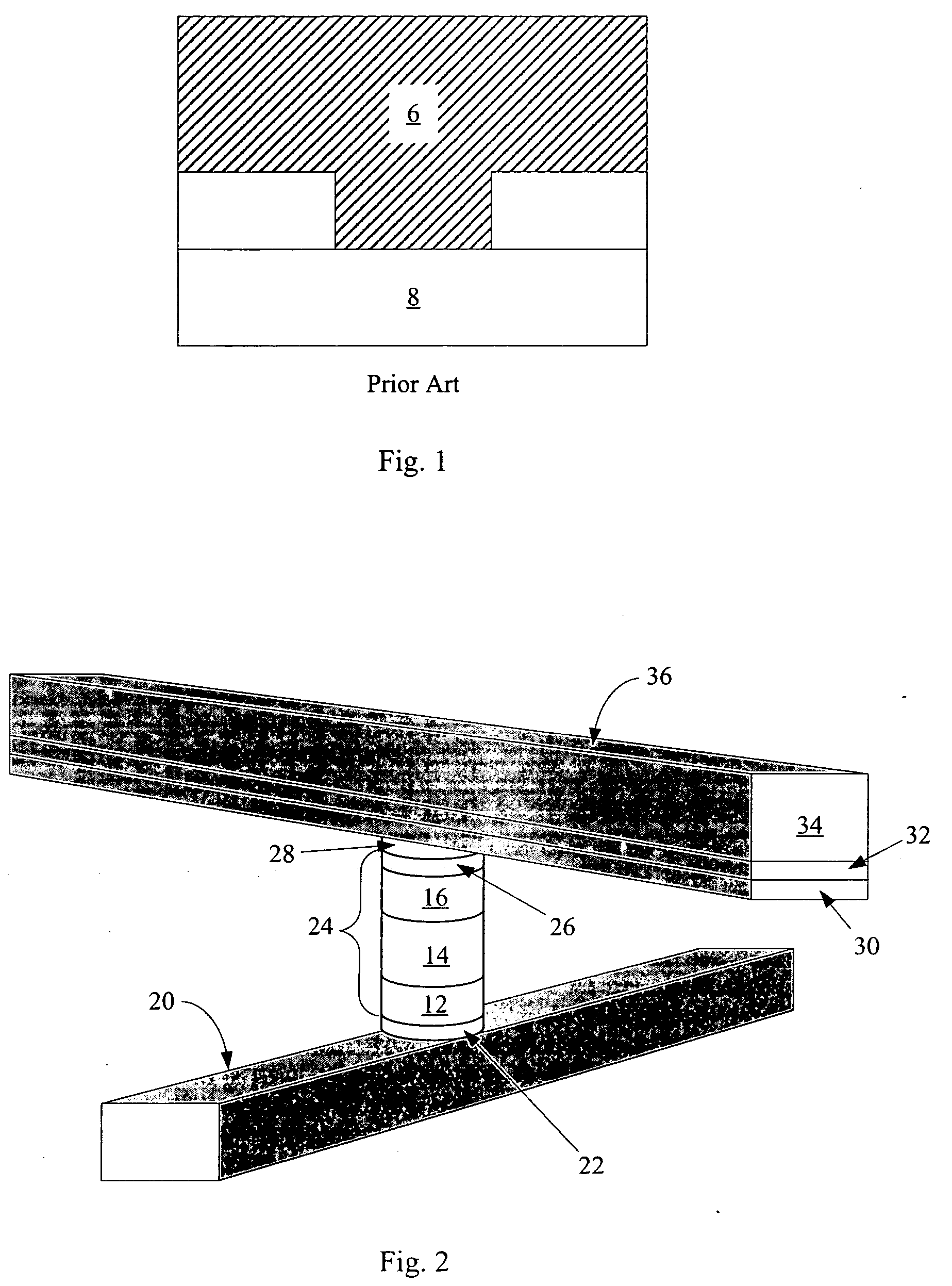
The invention provides for a nonvolatile memory cell comprising a dielectric material in series with a phase change material, such as a chalcogenide. Phase change is achieved in chalcogenide memories by thermal means. Concentrating thermal energy in a relatively small volume assists this phase change. By applying high voltage across a dielectric layer, dielectric breakdown occurs, forming a low-resistance rupture region traversing the dielectric layer. This rupture region can serve to concentrate thermal energy in a phase-change memory cell. In a preferred embodiment, such a cell can be used in a monolithic three dimensional memory array.

Description

RELATED APPLICATIONS [0001] This application is a continuation-in-part of Herner et al., U.S. patent application Ser. No. 10 / 855,784, “An Improved Method for Making High-Density Nonvolatile Memory,” filed May 26, 2004; which is a continuation of Herner et al., U.S. patent application Ser. No. 10 / 326,470, “An Improved Method for Making High-Density Nonvolatile Memory,” filed Dec. 19, 2002 (since abandoned) and hereinafter the '470 application, both assigned to the assignee of the present invention and hereby incorporated by reference in their entirety. [0002] This application is related to Scheuerlein, U.S. application Ser. No. ______, “Structure and Method for Biasing Phase Change Memory Array for Reliable Writing,” (attorney docket number MA-132); to Scheuerlein, U.S. application Ser. No. ______ “A Non-Volatile Phase Change Memory Cell Having a Reduced Thermal Contact Area,” (attorney docket number MA-133); and to Scheuerlein, U.S. application Ser. No. ______, “A Write-Once Nonvola...

Claims


Application Information

Patent Timeline
Patent Type & Authority Applications(United States)
IPC IPC(8): G11C7/00G11C11/39G11C17/16H01L21/336H01L21/82H01L27/24H01L29/73H01L45/00
CPCG11C5/02H01L27/2481G11C13/00G11C13/0004G11C13/0069G11C17/16G11C2013/008G11C2213/71G11C2213/72G11C2213/77H01L45/06H01L45/12H01L45/1233H01L45/126H01L45/144H01L27/2409G11C11/39H10B63/84H10B63/20H10N70/801H10N70/8413H10N70/231H10N70/8828H10N70/826
Inventor SCHEUERLEIN, ROY E.HERNER, S. BRAD
Owner SANDISK TECH LLC
Learn More