Semiconductor device for detecting memory failure and method thereof

a technology of memory failure and semiconductor devices, applied in the direction of instrumentation, digital storage, engine seals, etc., can solve problems such as memory failur

Inactive Publication Date: 2005-07-21
SAMSUNG ELECTRONICS CO LTD
View PDF6 Cites 13 Cited by
  • Summary
  • Abstract
  • Description
  • Claims
  • Application Information

AI Technical Summary

Benefits of technology

[0024] Another exemplary embodiment of the present invention is a semiconductor device for testing memory, including a BIST controller for testing a plurality of memory devices, an address and control signal generator for generating address and control signals for reading data from the plurality of memory devices

Problems solved by technology

In all of the above described conventional devices, a comparison re

Method used


Image

  • Semiconductor device for detecting memory failure and method thereof
  • Semiconductor device for detecting memory failure and method thereof
  • Semiconductor device for detecting memory failure and method thereof

Examples


Embodiment Construction

[0027] Hereinafter, exemplary embodiments of the present invention will be described in detail with reference to the accompanying drawings.

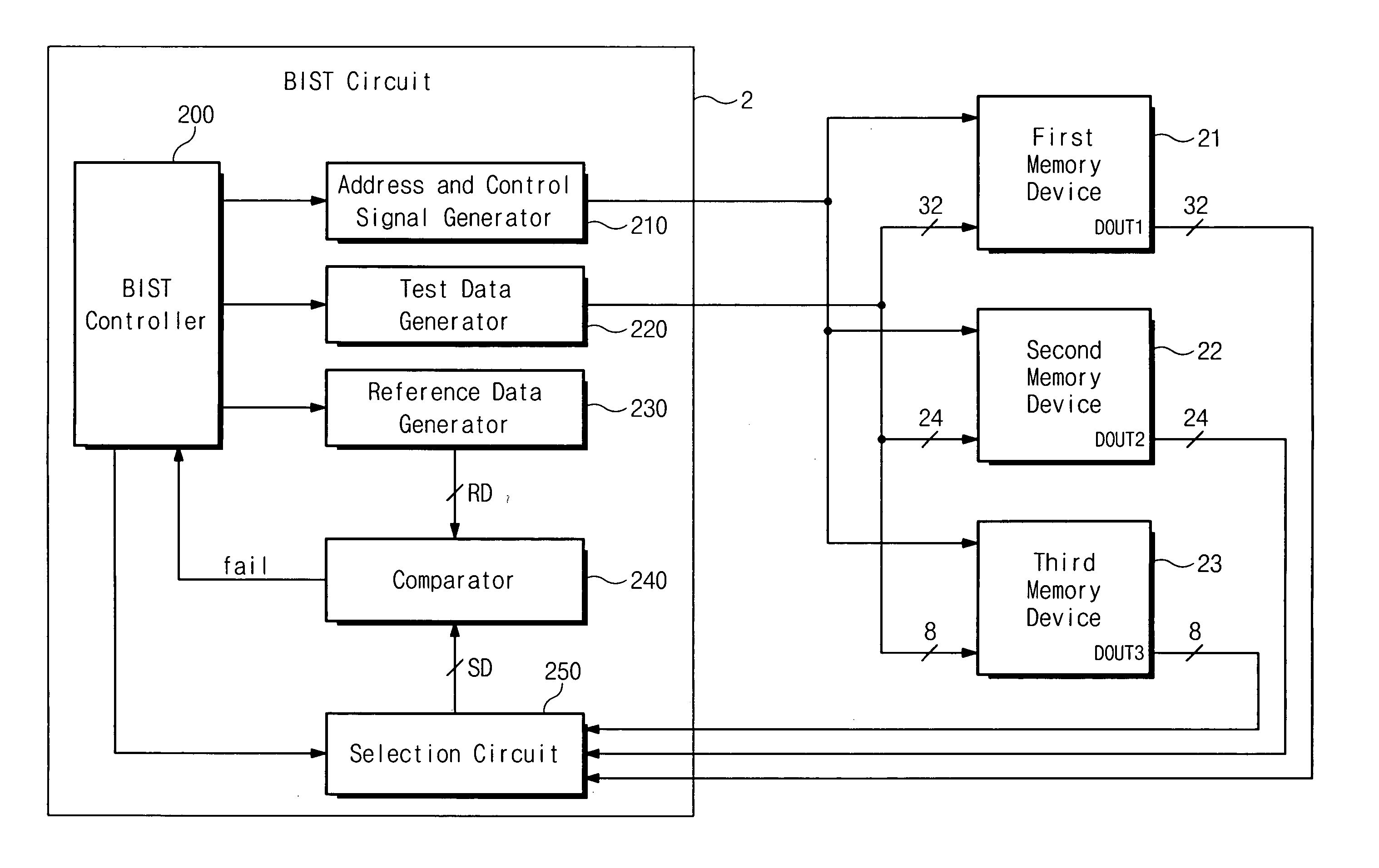
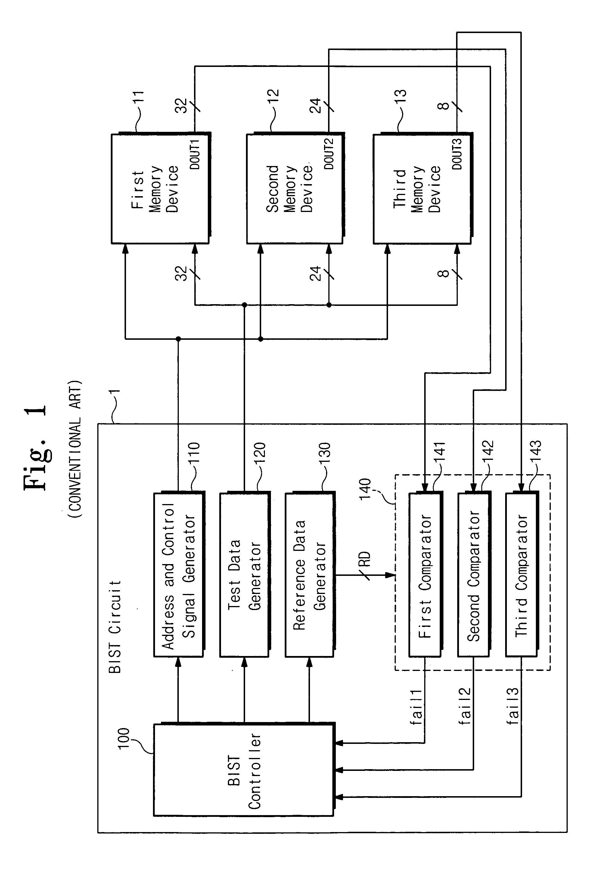
[0028]FIG. 2 illustrates a schematic block diagram of a BIST circuit for testing memory according to an exemplary embodiment of the present invention. Referring to FIG. 2, the BIST circuit may include a BIST controller 200, an address and control signal generator 210, a test data generator 220 a reference data generator 230, a comparator 240 and a selection circuit 250.

[0029] The BIST controller 200, the address and control signal generator 210, the test data generator 220 and the reference data generator 230 may function similarly as compared to the BIST controller 100, address and control signal generator 110, and test data generator 120, respectively, of FIG. 1.

[0030] In an exemplary embodiment of the present invention, the selection circuit 250 may select one of the first memory device 21, second memory device 22, and third memory device 2...


PUM


Abstract

A semiconductor device for testing memory, including a BIST controller for testing a plurality of memory devices, an address and control signal generator for generating address and control signals for reading data from the plurality of memory devices, a test data generator for generating test data, and a fail detector for determining memory failure. Another semiconductor device for testing at least one of a plurality of memory devices, including a BIST controller for testing a plurality of memory devices, an address and control signal generator for generating address and control signals for reading data from the plurality of memory devices, a test data generator for generating test data, a reference data generator for generating reference data, and a fail detector for determining memory failure. A method of determining memory failure, including writing data to a plurality of memory devices, reading the data from the plurality of memory devices, comparing corresponding addresses of the read data simultaneously, outputting a single fail signal when the comparing step determines at least one of the read data from the plurality of memory devices as not being equal. A semiconductor device for testing memory, including a BIST controller for testing a plurality of memory devices, an address and control signal generator for generating address and control signals for reading data from the plurality of memory devices, a test data generator for generating test data, a reference data generator for generating reference data, a selection circuit for selecting the read data from one of the plurality of memory devices, and a comparator for comparing the read data from one of the plurality of memory devices with the reference data. A semiconductor device for testing memory, including a BIST controller for testing a plurality of memory devices, an address and control signal generator for generating address and control signals for reading data from the plurality of memory devices, a test data generator for generating test data, and a single comparison unit for determining memory failure in at least two of the plurality of memory devices. A method of determining memory failure, including writing data to a plurality of memory devices, reading the data from the plurality of memory devices, comparing corresponding addresses of the read data of at least two of the plurality of memory devices in a single comparison unit.

Description

CROSS REFERENCE TO RELATED APPLICATIONS [0001] This application claims the priority of Korean Patent Application 2004-02998 filed on Jan. 15, 2004, in the Korean Intellectual Property Office, the disclosure of which is incorporated herein by reference in its entirety. BACKGROUND OF THE INVENTION [0002] 1. Field of the Invention [0003] The present invention relates generally to semiconductor devices, and more particularly, to a semiconductor device for detecting memory failure. [0004] 2. Description of Prior Art [0005] Built-In Self-Test (BIST) circuits are self-diagnostic circuits for testing semiconductor memory devices. Test data may be applied to a BIST circuit in order to test semiconductor memory devices. The BIST circuit may compare data read from the semiconductor memory device with reference data, and may determine whether a memory failure exists in the semiconductor memory deviced based on the comparison. As memory sizes increase in semiconductor memory devices, an increase...

Claims


Application Information

Patent Timeline
IPC IPC(8): F16J15/08F02F11/00G11C5/00G11C29/26G11C29/40
CPCG11C29/26G11C2029/2602G11C2029/0405G11C29/40
Inventor LEE, HOI-JIN
Owner SAMSUNG ELECTRONICS CO LTD
Why Eureka
Try Eureka