
Sample inspection system

a technology of sample inspection and inspection system, which is applied in the field of sample inspection system, can solve problems such as surface breaking defects in semiconductor wafers, potential detriment to the performance of semiconductor chips made from wafers with such defects, and surface breaking defects in wafers

Inactive Publication Date: 2005-06-23
KLA TENCOR TECH CORP
View PDF51 Cites 11 Cited by
  • Summary
  • Abstract
  • Description
  • Claims
  • Application Information

AI Technical Summary

Benefits of technology

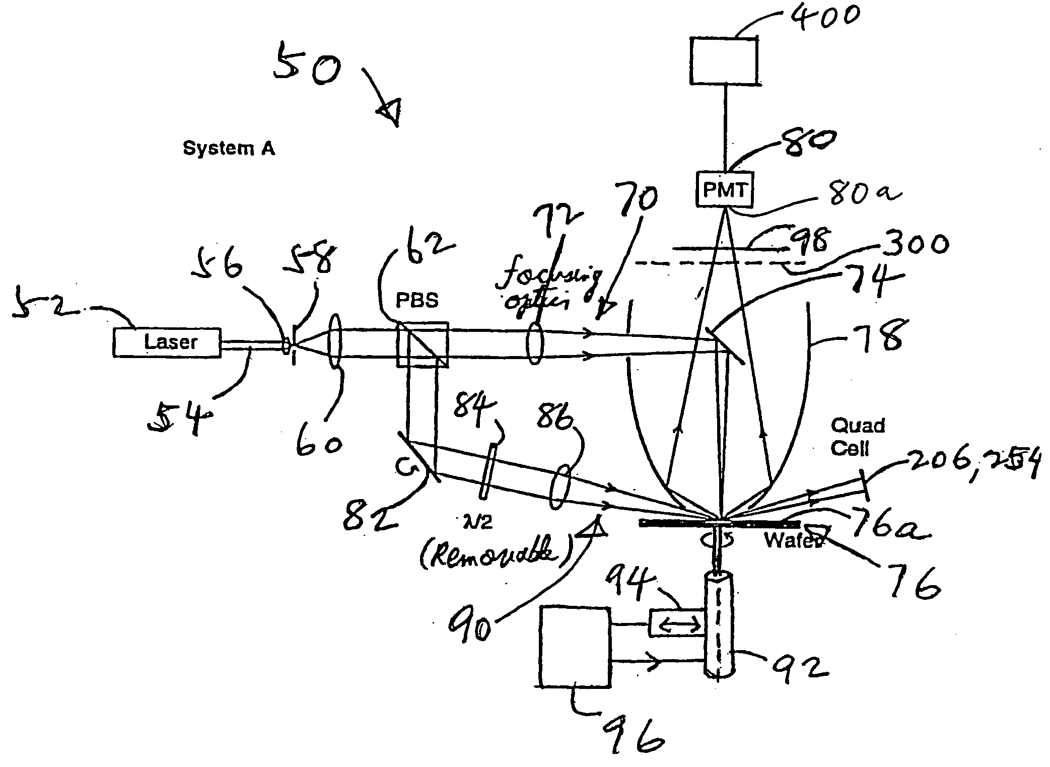
The invention is about an optical system and method for detecting anomalies on a sample surface. The system uses a combination of beams of radiation that are directed onto the surface and scattered radiation from the surface to detect particles and COPs (coating defects). The system distinguishes between particles and COPs by analyzing the difference in the sensitivity of the detection to surface particles and COPs. The system can also use a mirrored surface to receive scattered radiation and a detector to collect the scattered radiation. The technical effect of the invention is to provide a more sensitive and accurate method for detecting surface anomalies.

Problems solved by technology

COPs are surface breaking defects in semiconductor wafers which have been classified as particles due to inability of conventional inspection systems to distinguish them from real particles.
Another issue which has great significance in wafer inspection is that of COPs.
These are surface-breaking defects in the wafer.
According to some opinions in the wafer inspection community, such defects can cause potential detriments to the performance of semiconductor chips made from wafers with such defects.

Method used


Image

  • Sample inspection system
  • Sample inspection system
  • Sample inspection system

Examples


Embodiment Construction

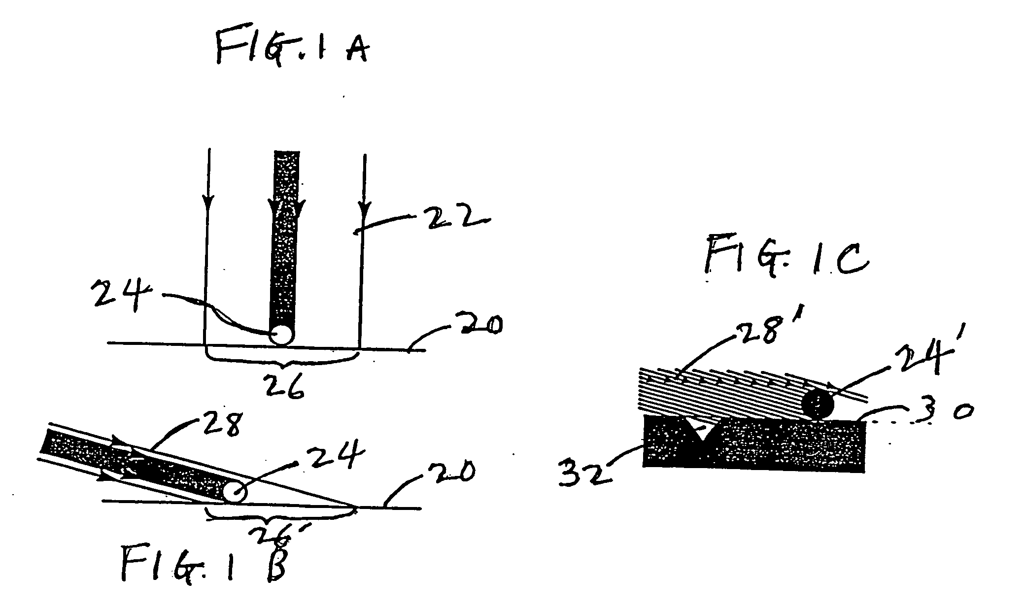
[0033]FIG. 1A is a schematic view of a surface 20 of a sample to be inspected and an illumination beam 22 directed in a direction normal to surface 20 to illuminate the surface and a particle 24 on the surface. Thus, the illumination beam 22 illuminates an area or spot 26 of surface 20 and a detection system (not shown) detects light scattered by particle 24 and by portion or spot 26 of the surface 20. The ratio of the photon flux received by the detector from particle 24 to that from spot 26 indicates the sensitivity of the system to particle detection.

[0034] If an illumination beam 28 directed at an oblique angle to surface 20 is used to illuminate spot 26′ and particle 24 instead, as shown in FIG. 1B, from a comparison between FIGS. 1A and 1B, it will be evident that the ratio of the photon flux from the particle 24 to that from the illuminated spot will be greater in the case of the oblique illumination in FIG. 1B compared to that in FIG. 1A. Therefore, for the same throughput ...


PUM

PropertyMeasurementUnit
wavelengthaaaaaaaaaa
wavelength λ2aaaaaaaaaa

Abstract

A curved mirrored surface is used to collect radiation scattered by a sample surface and originating from a normal illumination beam and an oblique illumination beam. The collected radiation is focused to a detector. Scattered radiation originating from the normal and oblique illumination beams may be distinguished by employing radiation at two different wavelengths, by intentionally introducing an offset between the spots illuminated by the two beams or by switching the normal and oblique illumination beams on and off alternately. Beam position error caused by change in sample height may be corrected by detecting specular reflection of an oblique illumination beam and changing the direction of illumination in response thereto. Butterfly-shaped spatial filters may be used in conjunction with curved mirror radiation collectors to restrict detection to certain azimuthal angles.

Description

BACKGROUND OF THE INVENTION [0001] This invention relates in general to sample inspection systems and, in particular, to an improved inspection system with good sensitivity for particles as well as crystal-originated-particles (COPs). COPs are surface breaking defects in semiconductor wafers which have been classified as particles due to inability of conventional inspection systems to distinguish them from real particles. [0002] Systems for inspecting unpatterned wafers or bare wafers have been proposed. See for example, PCT Patent Application No. PCT / US96 / 15354, filed on Sep. 25, 1996, entitled “Improved System for Surface Inspection.” Systems such as those described in the above-referenced application are useful for many applications, including the inspection of bare or unpatterned semiconductor wafers. Nevertheless, it may be desirable to provide improved sample inspection tools which may be used for inspecting not only bare or unpatterned wafers but also rough films. Another iss...

Claims


Application Information

Patent Timeline
Patent Type & Authority Applications(United States)
IPC IPC(8): G01N21/21G01N21/47G01N21/95
CPCG01N21/21G01N21/47G01N21/9501G01N2021/8848G01N2021/8825G01N2021/8845G01N21/956
Inventor VACZ-IRAVANI, MEHDISTOKOWSKI, STANLEYZHAO, GUOHENG
Owner KLA TENCOR TECH CORP
Learn More