
Image signal processing device, image signal processing method, electro-optical device, and electronic apparatus

a technology of image signal and processing method, applied in the field of image signal correction, can solve the problems of image signal transmitted through the image signal line, waveform distortion or phase delay of image signal, and the difference between a predetermined grayscale level and a grayscale level that is actually displayed, etc., to suppress display irregularities, reduce the number of shift register stages, and reduce the operating frequency required for the data line driving circui

Inactive Publication Date: 2005-06-23
SEIKO EPSON CORP
View PDF6 Cites 14 Cited by
  • Summary
  • Abstract
  • Description
  • Claims
  • Application Information

AI Technical Summary

Benefits of technology

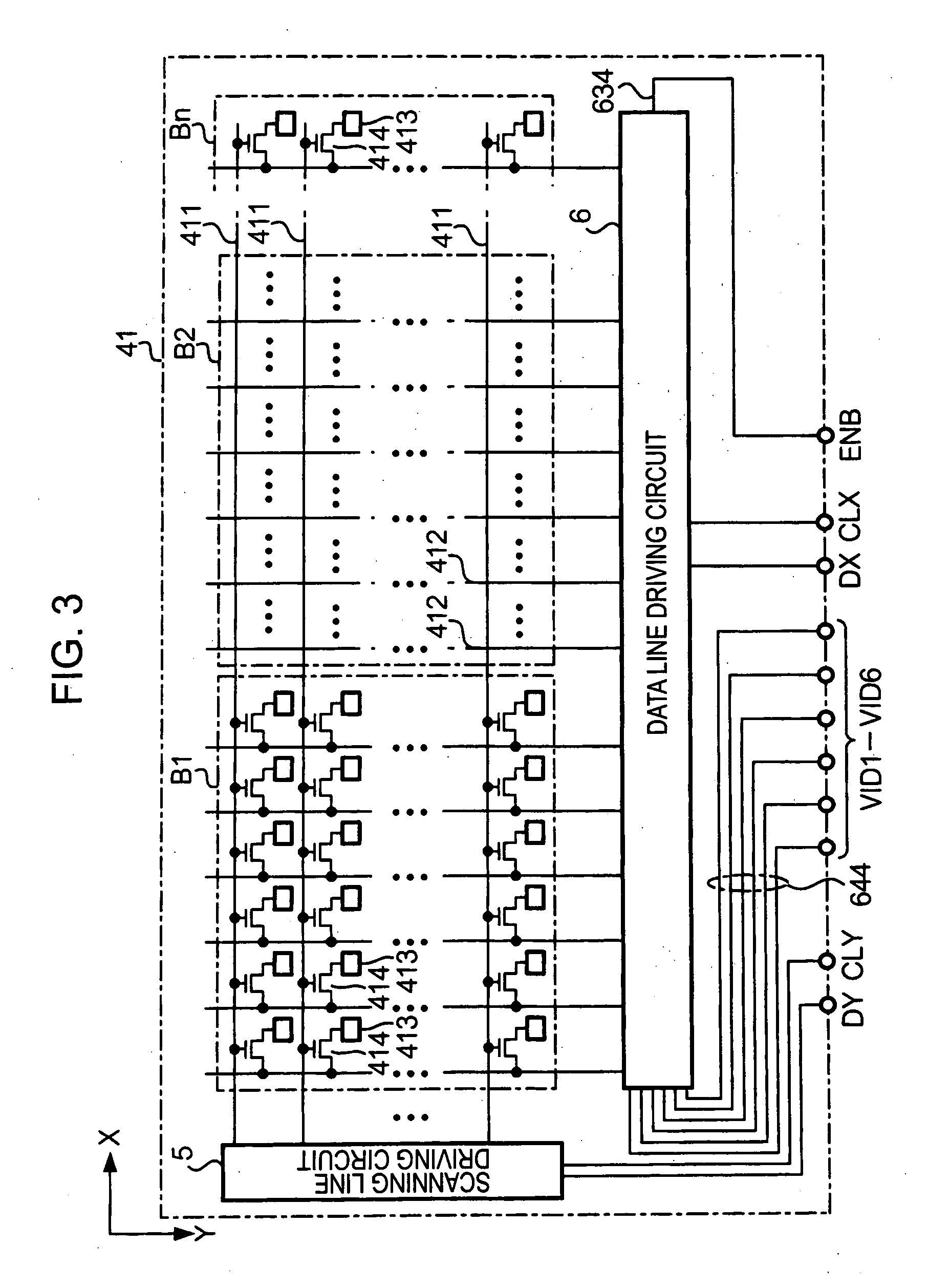
[0005] However, according to the above-mentioned structure, there is a problem in that the difference between a predetermined grayscale level and a grayscale level that is actually displayed, is changed along the extending direction of the image signal line. For example, even when the image signal is selected such that all pixels are displayed at the same grayscale level, a voltage applied to the pixel electrode located at the downstream side of the image signal line in the transmission direction of the image signal, is smaller than a voltage applied to the pixel electrode located at the upstream side thereof. In this case, in a liquid crystal device of a normally white mode, the grayscale of the pixel becomes brighter as the pixel is located nearer to the downstream side in the transmission direction of the image signal. Such a difference in grayscale is perceived as display irregularity (shades of a display color) by an observer, which causes the deterioration of display quality. Exemplary embodiments of the present invention are designed to address and / or solve the above-mentioned and / or other problems, and it is an object of exemplary embodiments of the present invention to remove display irregularity, thereby enhancing display quality.

Problems solved by technology

However, according to the above-mentioned structure, there is a problem in that the difference between a predetermined grayscale level and a grayscale level that is actually displayed, is changed along the extending direction of the image signal line.
Such a difference in grayscale is perceived as display irregularity (shades of a display color) by an observer, which causes the deterioration of display quality.
That is, the image signal transmitted through the image signal line may have waveform distortion or phase delay caused by the parasitic capacitance and resistance of the image signal line.
The level of the image signal supplied to the respective pixel electrodes varies due to a difference in the degree of signal distortion, which results in display irregularity.

Method used


Image

  • Image signal processing device, image signal processing method, electro-optical device, and electronic apparatus
  • Image signal processing device, image signal processing method, electro-optical device, and electronic apparatus
  • Image signal processing device, image signal processing method, electro-optical device, and electronic apparatus

Examples


Embodiment Construction

[0028] Hereinafter, exemplary embodiments of the present invention will be described with reference to the accompanying drawings. In exemplary embodiments which will be described below, the present invention is applied to a liquid crystal device in which liquid crystal is used as an electro-optical material, but the exemplary embodiments of the present invention are not limited to this type of liquid crystal device. That is, various exemplary modifications and variations thereof can be made without departing from the scope of the present invention. In addition, in the figures, which will be referred to in the following description, each component has different dimension and reduced scale from its actual dimension and reduced scale so as to be easily viewed in the figures.

[0029] Liquid Crystal Device

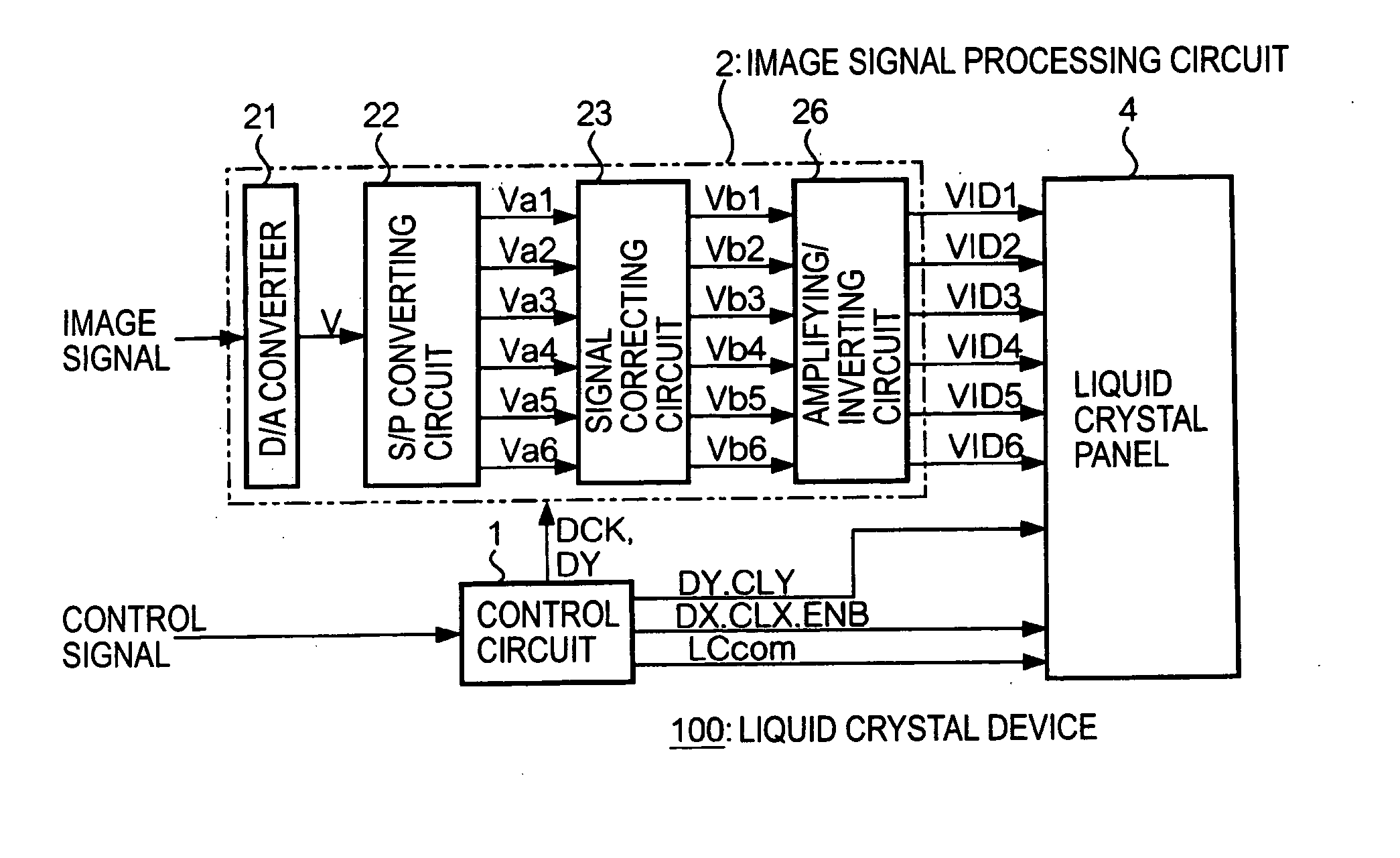
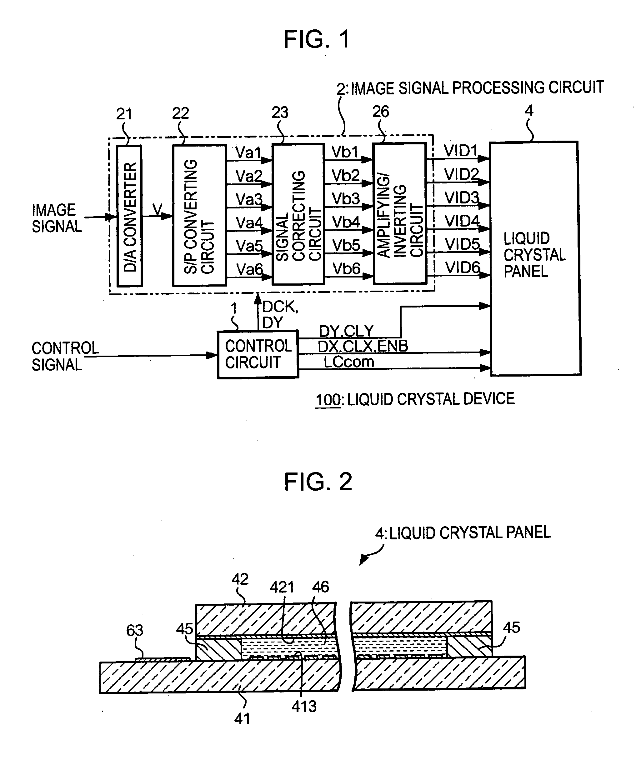
[0030]FIG. 1 is a schematic block diagram illustrating a functional structure of a liquid crystal device according to the present exemplary embodiment. As shown in FIG. 1, a liquid crys...


PUM

PropertyMeasurementUnit
angleaaaaaaaaaa
voltageaaaaaaaaaa
distanceaaaaaaaaaa

Abstract

Exemplary embodiments of the present invention reduce display irregularity in order to enhance display quality. A liquid crystal panel includes a plurality of pixel electrodes provided at intersections of a plurality of scanning lines and a plurality of data lines, a scanning line driving circuit to sequentially select the plurality of scanning lines, and a data line driving circuit to sample an image signal VID supplied to an image signal line that is provided in common to the plurality of data lines and to supply the sampled signal to each data line. A signal correcting circuit has a correction amount specifying circuit to specify a correction amount α of the image signal VID to be supplied to each data line based on the position of the data line with respect to the extending direction of the image signal line; and a correcting circuit to correct the image signal VID based on the correction amount α specified by the correction amount specifying circuit to supply the corrected image signal VID to the image signal line.

Description

BACKGROUND OF THE INVENTION [0001] 1. Field of Invention [0002] Exemplary embodiments of the present invention relate to a technique of correcting image signals in an electronic apparatus that displays an image using an electro-optical material, such as liquid crystal. [0003] 2. Description of Related Art [0004] The related art discloses various electro-optical devices that display images using an electro-optical material whose optical characteristics vary according to an electrical action. For example, related art document Japanese Unexamined Patent Application Publication No. 2002-149136 (see paragraphs 0005 to 0014 and FIG. 12) discloses an electro-optical device including pixel electrodes connected to scanning lines and data lines through switching elements, a scanning line driving circuit to sequentially select the scanning lines, an image signal line provided in common to the plurality of data lines, and a data line driving circuit to sample an image signal supplied to the ima...

Claims


Application Information

Patent Timeline
Patent Type & Authority Applications(United States)
IPC IPC(8): G09G3/20G02F1/133G09G3/30G09G3/36H01L51/50H04N5/66H05B33/14
CPCG09G3/3688G09G2320/0233G09G2320/0223G09G2310/0297G09G3/36
Inventor AOKI, TORU
Owner SEIKO EPSON CORP
Learn More