Storage device

a storage device and storage technology, applied in the field of storage devices, can solve the problems of increasing power consumption, failure to hold written data in a stable manner, etc., and achieve the effects of reducing power consumption, increasing or reducing the area of storage, and holding stably

Active Publication Date: 2005-06-09
SONY CORP
View PDF3 Cites 17 Cited by
  • Summary
  • Abstract
  • Description
  • Claims
  • Application Information

AI Technical Summary

Benefits of technology

[0012] In the storage device according to an embodiment of the present invention, an oxidation or a reduction of the oxidation-reduction active material depending on the application state of the voltage to the first and the second electrodes causes the electrode reaction inhibition layer to be formed along the interface region between the second electrode and the inter-electrode material layer or to disappear or alternatively, to increase or decrease the area thereof. The electrical characteristics between the first electrode and the second electrode vary depending on whether or not the electrode reaction inhibition layer exists at all or a difference in the area thereof, thereby allowing binary or more data to be stored in stable manner.
[0013] According to the storage device of the embodiments of the present invention, since the electrode reaction inhibition layer is formed along the interface region between the second electrode and the inter-electrode material layer or is allowed to disappear, or alternatively, increases or decreases the area thereof depending on the application condition of the voltage to the first and the second electrodes, the electrical characteristics between the first electrode and the second electrode vary depending on whether or not of the electrode reaction inhibition layer exists or a difference in the area thereof, thereby allowing the binary or more data to be stored in stable manner. The electrode reaction inhibition layer is formed by the oxidation of the oxidation-reduction active material. Accordingly, the layer is chemical stable, and as a result, the written data is held stably for a long period of time. Further, in the embodiments of the present invention, unlike the related art, there is no need to form an electron conduction channel made of silver, and the formation or the disappearance of an insulation film (the electrode reaction inhibition layer) is merely needed. Accordingly, the writing or the erasure of data may be achieved with a current of a smaller magnitude, whereby resulting in a considerable reduction of a power consumption.

Problems solved by technology

However, the storage element of the above structure of related art has some shortcoming on element characteristics in which a resistance value changes with a lapse of time, whereby leading to a failure to hold written data in stable manner. FIG. 13 shows changes of the resistance value over a lapse of time after the writing in the above storage element of related art in a case where the writing having been performed so as to satisfy a resistance state as low as a resistance value of 1 KΩ.
More specifically, it requires the large current at the time of the writing, thereby resulting in an increase of power consumption.

Method used


Image

  • Storage device
  • Storage device
  • Storage device

Examples


first embodiment

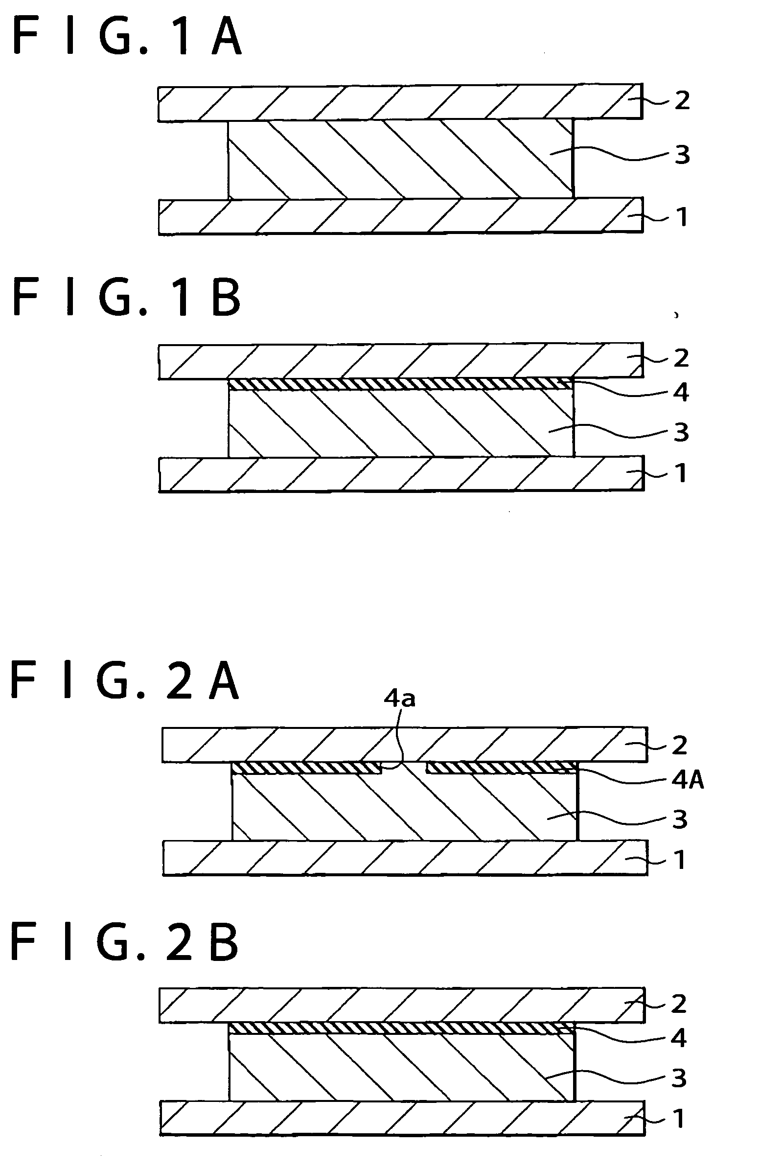
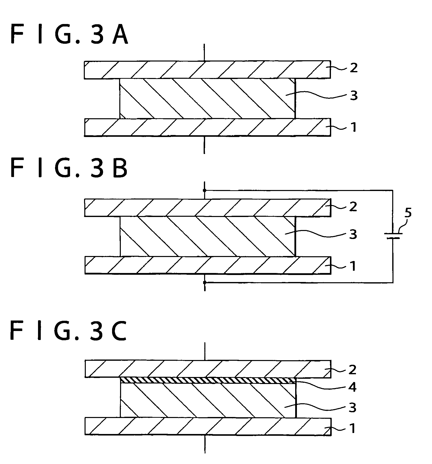
[0029] FIGS. 1(A) and 1(B) show a main configuration of a storage device according to a first embodiment of the present invention. Although it is not shown in the figure, the storage device includes a plurality of storage elements that may be, for example, arranged in a matrix form. The storage element has a structure having an inter-electrode material layer 3 sandwiched between a pair of electrodes 1 and 2 (a first and a second electrodes) facing each other, and is provided with a voltage application unit (not shown) for applying a predetermined voltage to the electrodes 1 and 2. Each of the plurality of storage elements has, in a corresponding arrangement, an active element or a transistor (not shown in the figure) for controlling electrical access to each element, thereby completing the configuration of the memory cell. Each storage element contains an oxidation-reduction active material A extended in a range over which an electric field produced at the time of an application of ...

second embodiment

[0043]FIG. 2(A) shows a second embodiment of the present invention, in which the element with the structure shown in FIG. 1(A) has the electrode reaction inhibition layer 4A with an opening 4a in a part thereof. The electrode reaction inhibition layer 4A including the above electrode reaction inhibition material B (nickel oxide (NiO) in this case) is formed in advance on a surface of one of the electrodes, for example the second electrode 2.

[0044] The electrode reaction inhibition layer 4A may be obtained by, after a formation of the electrode reaction inhibition layer 4 (nickel oxide) over the whole surface of the electrode 2 in the element of the structure shown in FIG. 1(A) by oxidizing nickel contained in the electrode 2 by the application of a negative potential than that of the second electrode 2 to the electrode 1, applying a positive potential than that of the electrode 2 to the electrode 1. Thus, a part or most of the electrode reaction inhibition layer 4 is destroyed or d...

third embodiment

[0088] A third embodiment of the present invention is configured to form a Schottky diode between the electrode 2 and the inter-electrode material layer 3 in the structure shown in FIGS. 2(A) and 2(B), so that the inter-electrode material layer 3 is specified as a p-type semiconductor layer. The Schottky diode permits the current to flow if the application of a negative voltage larger than a threshold value of the diode characteristics to the electrode 2, and conversely, permits no flow of the current if the application of a positive voltage to the electrode 2. A specific material of the inter-electrode material layer 3 includes amorphous silicon (Si) containing a p-type impurity, for instance.

[0089] The electrode 1 is formed with a material such as gold (Au) capable of making an electrical contact with the semiconductor material described above. On the other hand, the electrode 2 is formed with the above oxidation-reduction active material A such as nickel (Ni). As described above...


PUM


Abstract

A storage device includes a first electrode, a second electrode facing the first electrode, an inter-electrode material layer provided between the first electrode and the second electrode, and a voltage application unit applying a predetermined voltage to the first and the second electrodes. Furthermore, an oxidation-reduction active material changeable into an electrode reaction inhibition layer by applying voltages to the first and the second electrodes is contained in a region that is covered by an electric field, the electric field being generated when the voltage is applied, and the electrode reaction inhibition layer is either formed along an interface region between the second electrode and the inter-electrode material layer, or changes an area thereof, or disappears depending on an application condition of the voltage to the first and the second.

Description

CROSS REFERENCES TO RELATED APPLICATIONS [0001] The present invention claims priority to its priority document No. 2003-404088 filed in the Japanese Patent Office on Dec. 3, 2003, the entire contents of which being incorporated by reference herein. BACKGROUND OF THE INVENTION [0002] 1. Field of the Invention [0003] The present invention relates to a storage device that is capable of performing a writing, a readout and an erasure of binary data (information) or data with more levels by changing electrical characteristics between two electrodes. [0004] 2. Description of the Related Art [0005] In related art, a micro electronic programmable element as shown in FIGS. 12(A) and 12(B) is known as a storage element that may be formed easily with a simple structure (see Japanese Patent Application Publication 2002-536840). This element ionizes, by an application of a predetermined voltage, silver (Ag) contained in an inter-electrode material layer 103 between two electrodes 101 and 102, and...

Claims


Application Information

Patent Timeline
IPC IPC(8): G11C13/02G11C16/04H01L27/10H01L31/109H01L45/00
CPCG11C13/0009H01L45/146G11C13/0069G11C2013/009G11C2213/15G11C2213/34G11C2213/51G11C2213/56G11C2213/72G11C2213/79H01L45/085H01L45/1233H01L45/1246H01L45/1266H01L45/144G11C13/0011H10N70/245H10N70/828H10N70/8416H10N70/826H10N70/8828H10N70/8833H01L27/10
Inventor ISHIDA, MINORUARATANI, KATSUHISAKOUCHIYAMA, AKIRATSUSHIMA, TOMOHITO
Owner SONY CORP
Why Eureka
Try Eureka