Edge transfer lithography
a technology of lithography and edge, applied in the field of edge transfer lithography, can solve the problems of expensive and sophisticated apparatus for their implementation, and achieve the effects of simple implementation, reduced feature size, and broad applicability of cp
- Summary
- Abstract
- Description
- Claims
- Application Information
AI Technical Summary
Benefits of technology
Problems solved by technology
Method used
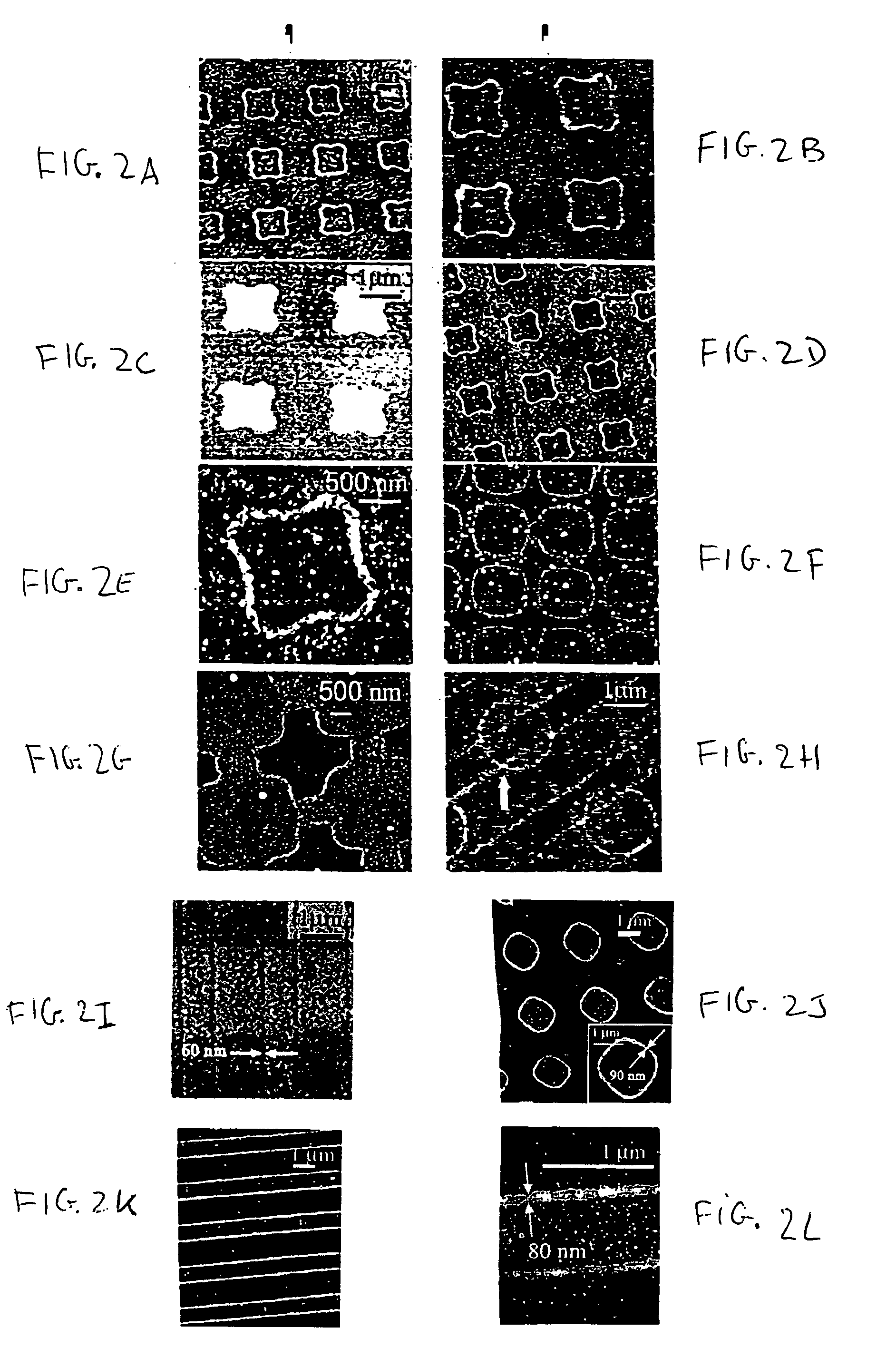
Image

Examples
example 1
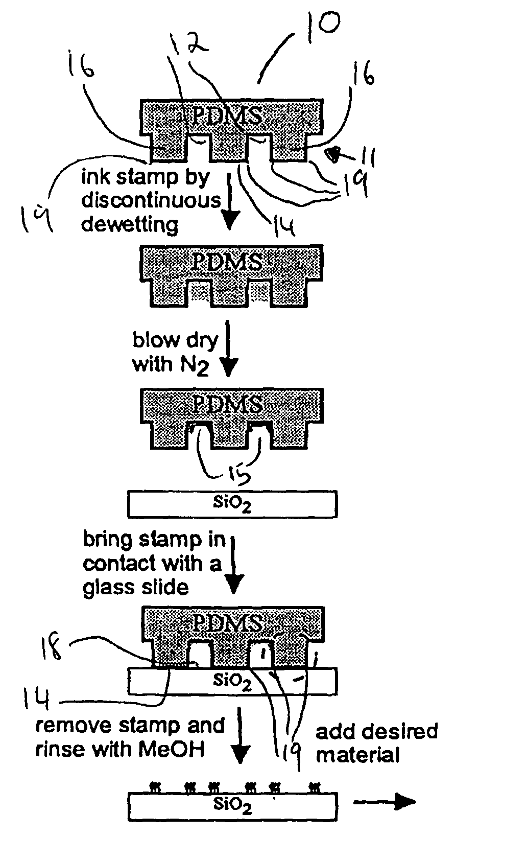
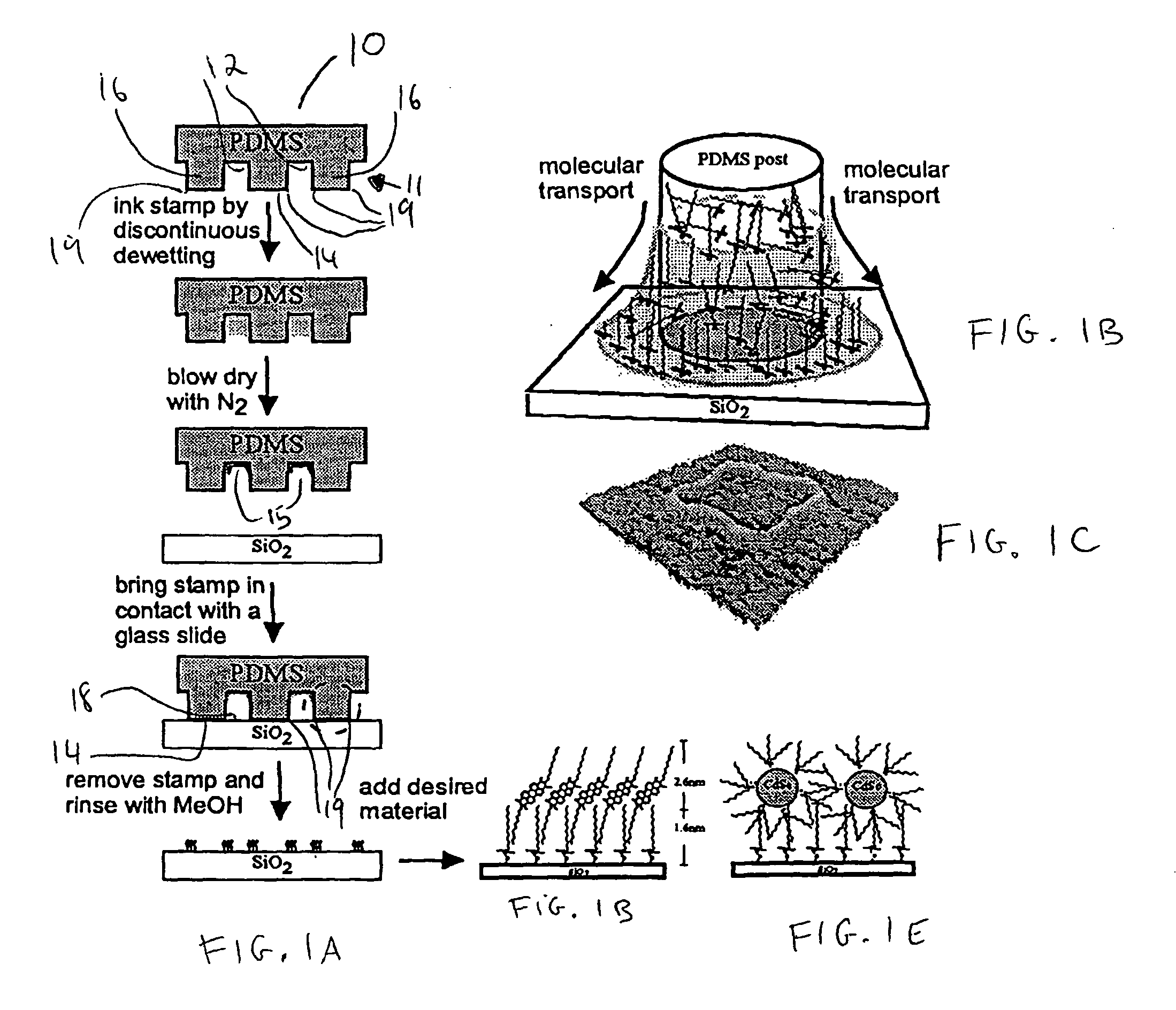
Application of Dimethyloctadecylmethoxy Silane (DOMS) to a Glass Surface
[0039] PDMS (Sylgard 184 Elastomer Kit, available from Dow Corning) stamps are molded on patterned silicon wafers using standard methods such as described in Xia, X., and Whitesides, G. M., “Soft lithography,” Angewandte Chemie International Edition in English, Vol. 37 (1998), pp. 550-74. The stamp is inked lightly with a 2% by volume solution of DOMS (90% pure used as purchased from Fluka) in anhydrous methanol or ethanol (both available from Aldrich) using a cotton swab. The residual solvent is removed by blow-drying with N2. The stamp is immediately brought in contact with a glass slide (available from Corning), freshly cleaned with piranha solution, which consists of 7:3 volume / volume 98% H2SO4 and 30% H2O2 No external pressure is applied to the stamp structure 10 or the substrate. The assembly is baked for ˜30 min at 70° C. after which the stamp is removed and the substrate is thoroughly rinsed with methan...
example 2
Application of Dimethyldodecylchlorosilane (DDCS) to a Glass Surface
[0040] The experiment is performed in the same way as in Example 1 but using DDCS (90% pure used as purchased from Fluka) instead of DOMS.
PUM
| Property | Measurement | Unit |
|---|---|---|
| Diameter | aaaaa | aaaaa |
| Pressure | aaaaa | aaaaa |
| Polarity | aaaaa | aaaaa |
Abstract
Description
Claims
Application Information
 - R&D
- Intellectual Property
- Life Sciences
- Materials
- Tech Scout
- Unparalleled Data Quality
- Higher Quality Content
- 60% Fewer Hallucinations
Browse by: Latest US Patents, China's latest patents, Technical Efficacy Thesaurus, Application Domain, Technology Topic, Popular Technical Reports.
© 2025 PatSnap. All rights reserved.Legal|Privacy policy|Modern Slavery Act Transparency Statement|Sitemap|About US| Contact US: help@patsnap.com