
Method and system of testing complex MCM's

a complex and complex technology, applied in the direction of electronic circuit testing, measurement devices, instruments, etc., can solve the problems of damage to the surrounding substrate, the efficiency and the inability of prior art cluster probe testers to efficiently test many mcm's

Inactive Publication Date: 2005-05-19
INTELLECTUAL DISCOVERY INC
View PDF9 Cites 4 Cited by
  • Summary
  • Abstract
  • Description
  • Claims
  • Application Information

AI Technical Summary

Benefits of technology

"The patent describes a system and method for testing electrical devices with multiple contact pads using a multi-probe tester. The test probes and device contact pads are arranged in a common distribution pitch, and a means for masking test probes prevents them from affecting the testing results. This means can be a physical mask or a software command that disregards the input from a test probe. The technical effect of this invention is to improve the accuracy and reliability of testing electrical devices with multiple contact pads."

Problems solved by technology

However, prior art step-and-repeat cluster-probe testing efficiency has limitations.
As it is common and desirable for an MCM to comprise chips with a plurality of divergent C4 patterns and / or footprint dimensions, the prior art cluster probe tester cannot efficiently test many MCM's.
These surrounding regions commonly have surface depth dimensions divergent from that of the chip, which may cause failure of the cluster probe to correctly interface the chip C4 pads, may cause damage to the surrounding substrate, or may cause the creation of residual debris by an extra the interaction of probe beams with the MCM on smaller chip sites.
The removal of residual debris is a significant and expensive problem for large-scale MCM production.
This is a high throughput electrical test method, but it requires a huge resource investment on tester and probe.
The product-specific manufacturing costs for such a full cluster probe test is enormous, perhaps in the neighborhood of five to six million dollars, and therefore not practical.
However, disadvantages occur from multi-hour cycle times when used on complex MCM substrates with very high net counts and the resulting high operational costs and high number of required testers to provide the necessary capacity.
This method does not require big investment on tooling, but it is a low throughput test method and cannot handle high volume production and is therefore not practical for large scale MCM production.

Method used


Image

  • Method and system of testing complex MCM's
  • Method and system of testing complex MCM's
  • Method and system of testing complex MCM's

Examples


Embodiment Construction

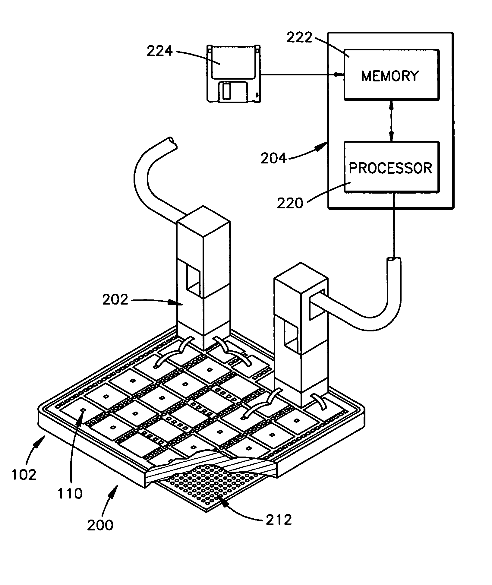
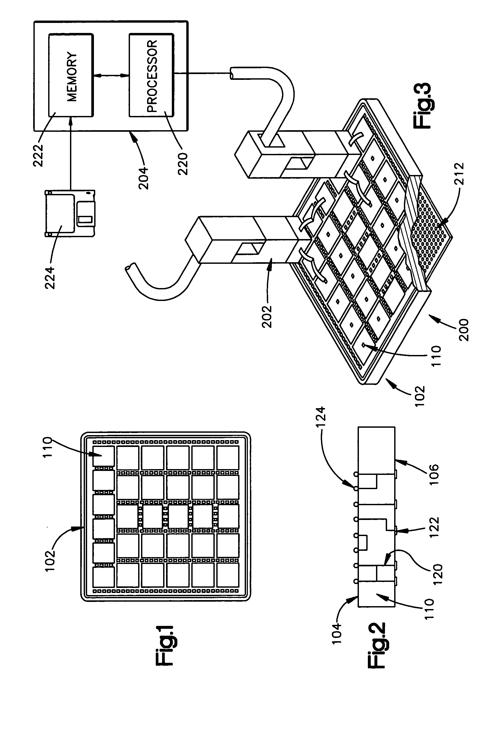
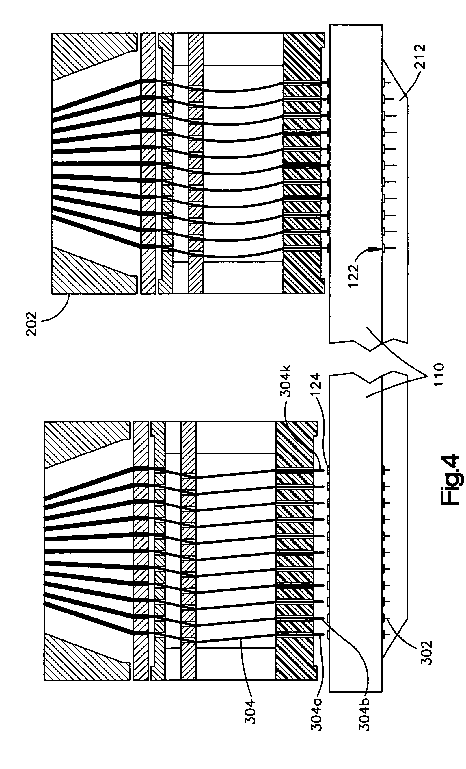
[0021] The present invention is a test method and system that utilizes “masking” methods with a conventional Step and Repeat Cluster Probe Tester to test complex MCM's comprising different size chips sharing a common pitch but with divergent C4 footprints with non-repeating C4 patterns. These types of complex MCM's thus have surface features that are not appropriate for testing through a normal stepable C4 pattern.

[0022] Referring now to FIG. 5, a self-locate mask 400 according to the present invention is shown. The mask provides a template that exposes only the chip features to be tested through a plurality of mask apertures 402. Each aperture 402 has a shape designed to expose only those chip areas to be tested to the cluster probe arm 202. For example, it is readily apparent from the drawings that aperture 402a has a much smaller opening area than that of 402b.

[0023] One embodiment of the mask 400 is manufactured from a sheet of Kapton™, made by Dupont, Inc., with thickness of ...


PUM


Abstract

A system and method for utilizing a multi-probe tester to test an electrical device having a plurality of contact pads. Multi-probe tester test probes and electrical device contact pads are arrayed in a common distribution pitch, and a means for masking test probes masks at least one test probe, thereby preventing the at least one test probe from returning a test result to the testing apparatus. In one embodiment the means for masking test probes is a mask membrane physically preventing at least one test probe from making contact with the electrical device. In another embodiment, the means for masking is at least one software command configured to cause an input from at least one test probe to be disregarded during a test routine. Another embodiment features both mask membrane and software command probe masking.

Description

FIELD OF THE INVENTION [0001] Methods and systems for testing electrical devices. More particularly, high throughput electrical test methods and systems for complex multi-chip computer system modules MCM's, more particularly step and repeat cluster probe testing of complex multilayer ceramic (MLC) substrates. BACKGROUND OF THE INVENTION [0002] An important trend in the electronics industry today is the use of multi-chip modules (MCMs). Simply defined, a MCM has multiple integrated circuits (ICs) packaged on an insulting substrate that interconnects the ICs and provides external connections. MCMs create functional islands using both custom and standard chips that can help provide improved system performance and smaller size and weight, while offering a cost-effective solution for many applications. [0003] One example of a high-performance MCM multichip substrate is the IBM Corporation S / 390™ product line. FIGS. 1 and 2 illustrate both form-factor and design information on one embodim...

Claims


Application Information

Patent Timeline
Patent Type & Authority Applications(United States)
IPC IPC(8): G01R31/28
CPCG01R31/2886
Inventor YU, YUET-YINGBODENWEBER, PAUL F.HENDRICKS, CHARLES J.SEELMANN, FRANK C.
Owner INTELLECTUAL DISCOVERY INC
Learn More