
Doping of organic opto-electronic devices to extend reliability

a technology of optoelectronic devices and organic elastomers, which is applied in the direction of discharge tube luminescnet screens, natural mineral layered products, other domestic articles, etc., to achieve the effect of enhancing the morphological stability of the host material

Active Publication Date: 2005-04-07
UNIVERSAL DISPLAY +1
View PDF26 Cites 42 Cited by
  • Summary
  • Abstract
  • Description
  • Claims
  • Application Information

AI Technical Summary

Benefits of technology

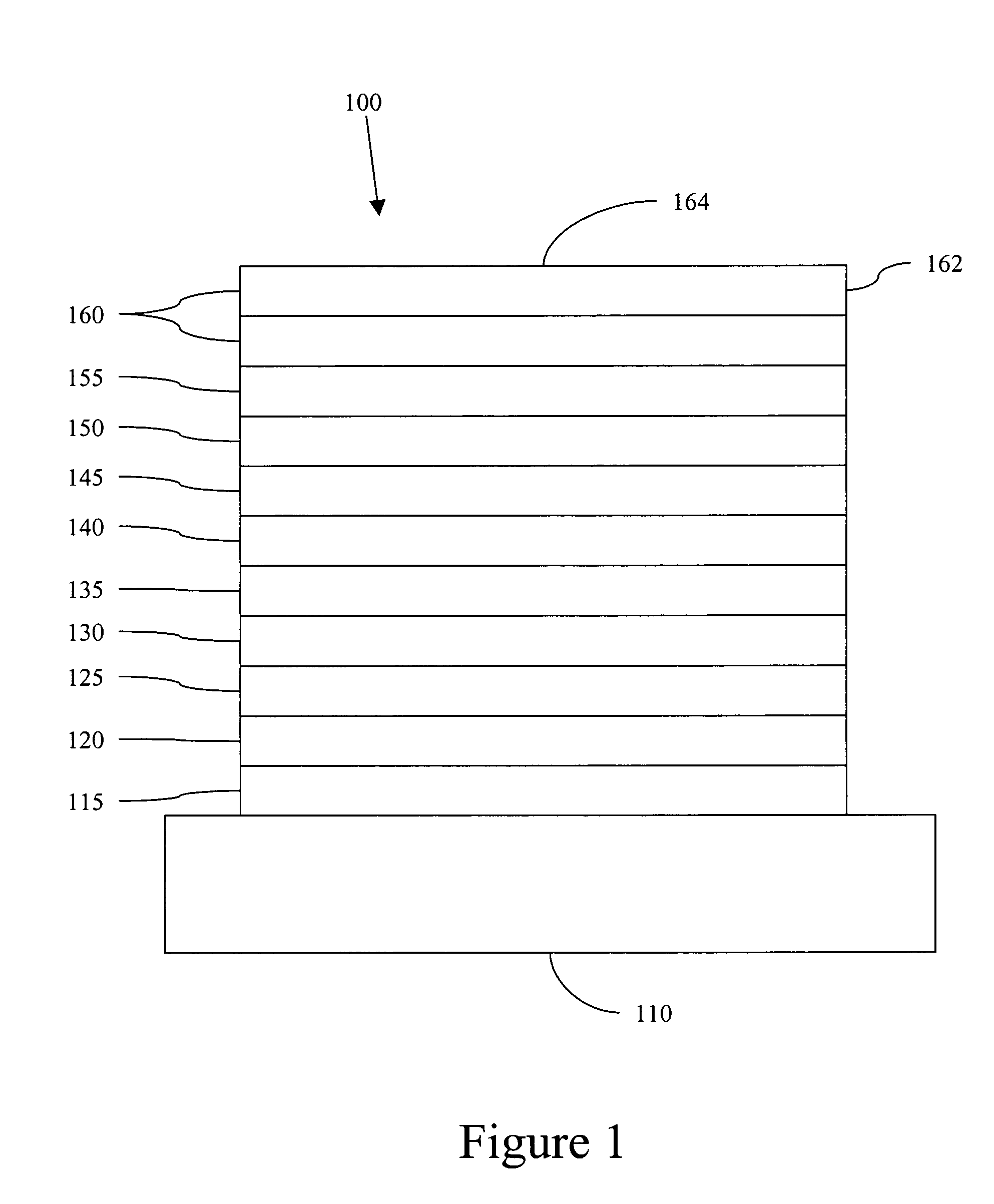
In one embodiment, the invention relates to an organic light emitting device comprising an anode, a cathode, a first organic layer disposed between and in electrical connection with the anode and the cathode, wherein the first organic layer is an emissive layer; and a second organic layer disposed between the first organic layer and the cathode or between the first organic layer and the anode. The second organic layer comprises a host material that is morphologically unstable and a dopant material that enhances the morphological stability of the host material. The dopant material is present in the host material at a concentration of 50% by weight or less. In one embodiment, the resulting device has a lifetime that is at least about 25% longer than an analogous device having a second organic layer that does not contain the dopant material. In another embodiment, the host material is a material that becomes at least 20% crystalline after 100 hours at 35° C. when deposited as a initially amorphous this film, and the mixture of the host material and the dopant material does not become more than 10% crystalline after 100 hours at 35° C. when deposited as a initially amorphous this film.

Problems solved by technology

This instability may be attributed to the deterioration of one or more of the organic layers.

Method used


Image

  • Doping of organic opto-electronic devices to extend reliability
  • Doping of organic opto-electronic devices to extend reliability
  • Doping of organic opto-electronic devices to extend reliability

Examples


example 1

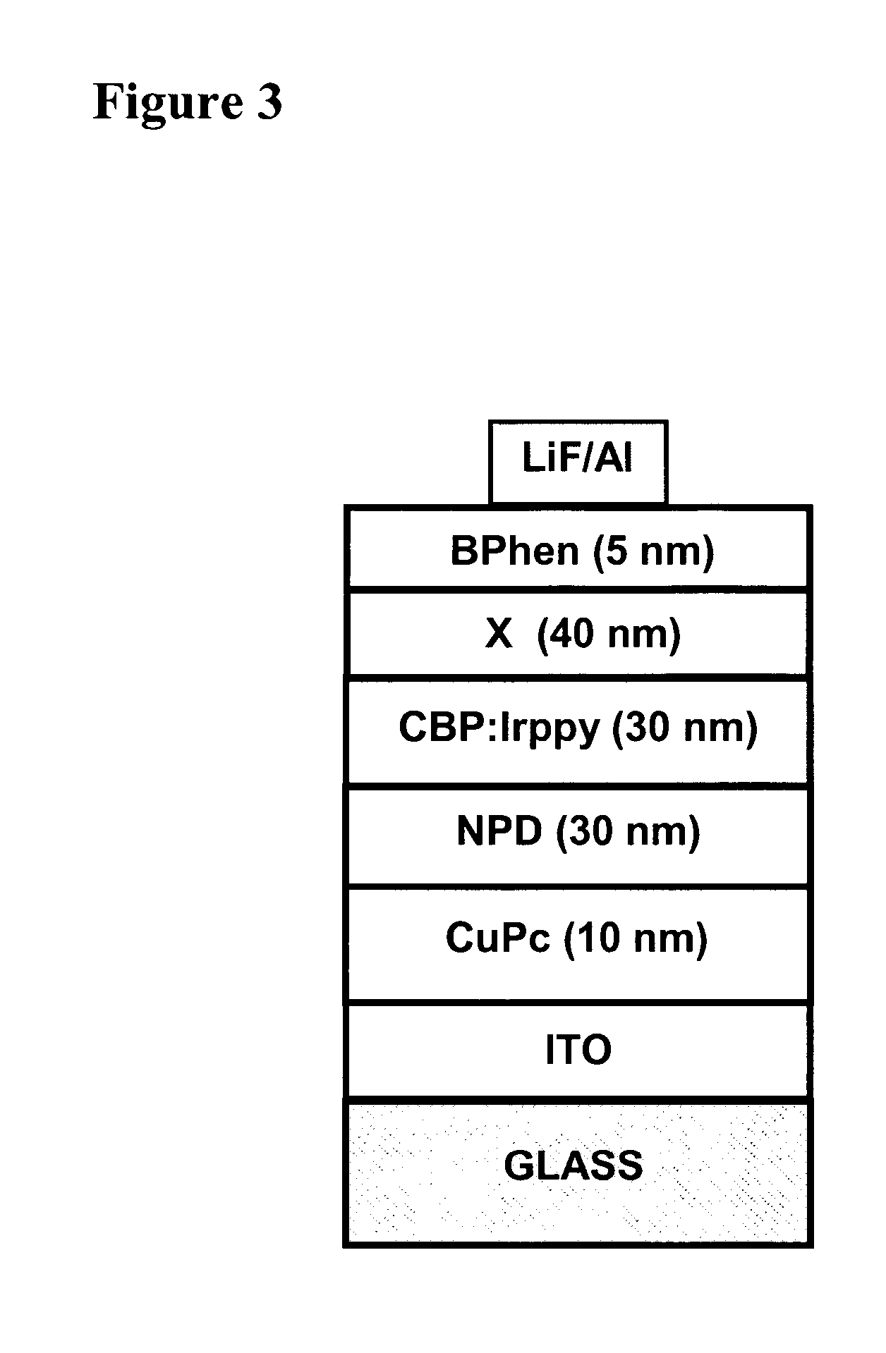
OLEDs were prepared with the device structure ITO / CuPc (10 nm) / NPD (30 nm) / CBP:Irppy (5 nm, 6%) / X / BPhen (5 nm) / LiF / Al. The device structure is shown in FIG. 3. The HBL (X) consisted of either BAlq, or 25 wt. % BPhen in BAlq, or 50 wt. % BPhen in BAlq. The copper phthalocyanine (CuPc) layer improves hole injection into the 4,4′-bis[N-(1-nathyl)-N-phenyl-amino]biphenyl (NPD) hole transport layer, and fac-tris(2-phenylpyridine) iridium (Irppy) was doped at 6 wt. % into a 4,4′-N,N′-dicarbazole-biphenyl (CBP) host.

The normalized luminance versus time characteristics of devices with the various mixtures of BAlq and BPhen is shown in FIG. 4. Device stability decreases as the concentration of BPhen is varied from 0 wt. % to 50 wt. %. Devices with X=BAlq, 25 wt. % BPhen:BAlq, and 50 wt. % BPhen:BAlq have t1 / 2=3900 hrs and 2600 hrs, respectively, and from an extrapolation of the curve to half the initial luminance (solid line) t1 / 2=10,000 hrs when X=BAlq. Normalized to L0=100 cd / m2, the li...


PUM

PropertyMeasurementUnit
Temperatureaaaaaaaaaa
Fractionaaaaaaaaaa
Fractionaaaaaaaaaa

Abstract

The present invention is directed to multi-layer organic devices having improved stability, wherein at least one layer of the device comprises a host material that is morphologically unstable and a dopant material that provides improved morphological properties to the layer. The layer may be incorporated into, for example, OLEDs, organic phototransistors, organic photovoltaic cells, and organic photodetectors.

Description

FIELD OF THE INVENTION The present invention relates to stable organic multilayer devices. More particularly, the invention relates to organic opto-electronic devices having improved stability. BACKGROUND Opto-electronic devices that make use of organic materials are becoming increasingly desirable for a number of reasons. Many of the materials used to make such devices are relatively inexpensive, so organic opto-electronic devices have the potential for cost advantages over inorganic devices. In addition, the inherent properties of organic materials, such as their flexibility, may make them well suited for particular applications such as fabrication on a flexible substrate. Examples of organic opto-electronic devices include organic light emitting devices (OLEDs), organic phototransistors, organic photovoltaic cells, and organic photodetectors. For OLEDs, the organic materials may have performance advantages over conventional materials. For example, the wavelength at which an org...

Claims


Application Information

Patent Timeline
IPC IPC(8): H01L51/00H01L51/30H01L51/40H01L51/42H01L51/50H01L51/54H05B33/12
CPCH01L51/002H01L51/0035H01L51/0051H01L51/0081H01L51/0085H01L51/42Y02E10/549H01L51/5048H01L51/5052H01L51/5096H01L2251/308Y10S428/917H01L51/5016H10K71/30H10K85/111H10K85/611H10K85/324H10K85/342H10K50/11H10K2101/10H10K50/14H10K50/155H10K50/165H10K50/18H10K2102/103H10K30/00
Inventor FORREST, STEPHEN R.D'ANDRADE, BRIAN WENDELLCHWANG, ANNA
Owner UNIVERSAL DISPLAY
Learn More