Display with micro pockets

a technology of micro-pockets and displays, applied in the field of displays, can solve the problems of the amount of electro-optic material that needs to be filled between the electrode layer and the substrate, and achieve the effects of reducing the number of layers, cost-effective production methods, and robust display

Inactive Publication Date: 2005-03-31
POLYDISPLAY AS
View PDF9 Cites 1 Cited by
  • Summary
  • Abstract
  • Description
  • Claims
  • Application Information

AI Technical Summary

Benefits of technology

[0008] The object of the present invention is to reduce the number of layers and a minimal use of electro-optical material, resulting in a more cost-effective production method and a robust display.

Problems solved by technology

One drawback with this display is the amount of electro-optic material needed to be filled between the electrode layer and the substrate.

Method used


Image

  • Display with micro pockets
  • Display with micro pockets
  • Display with micro pockets

Examples


Embodiment Construction

[0024] With reference to the figures, the following detailed description explains how the invention is obtained.

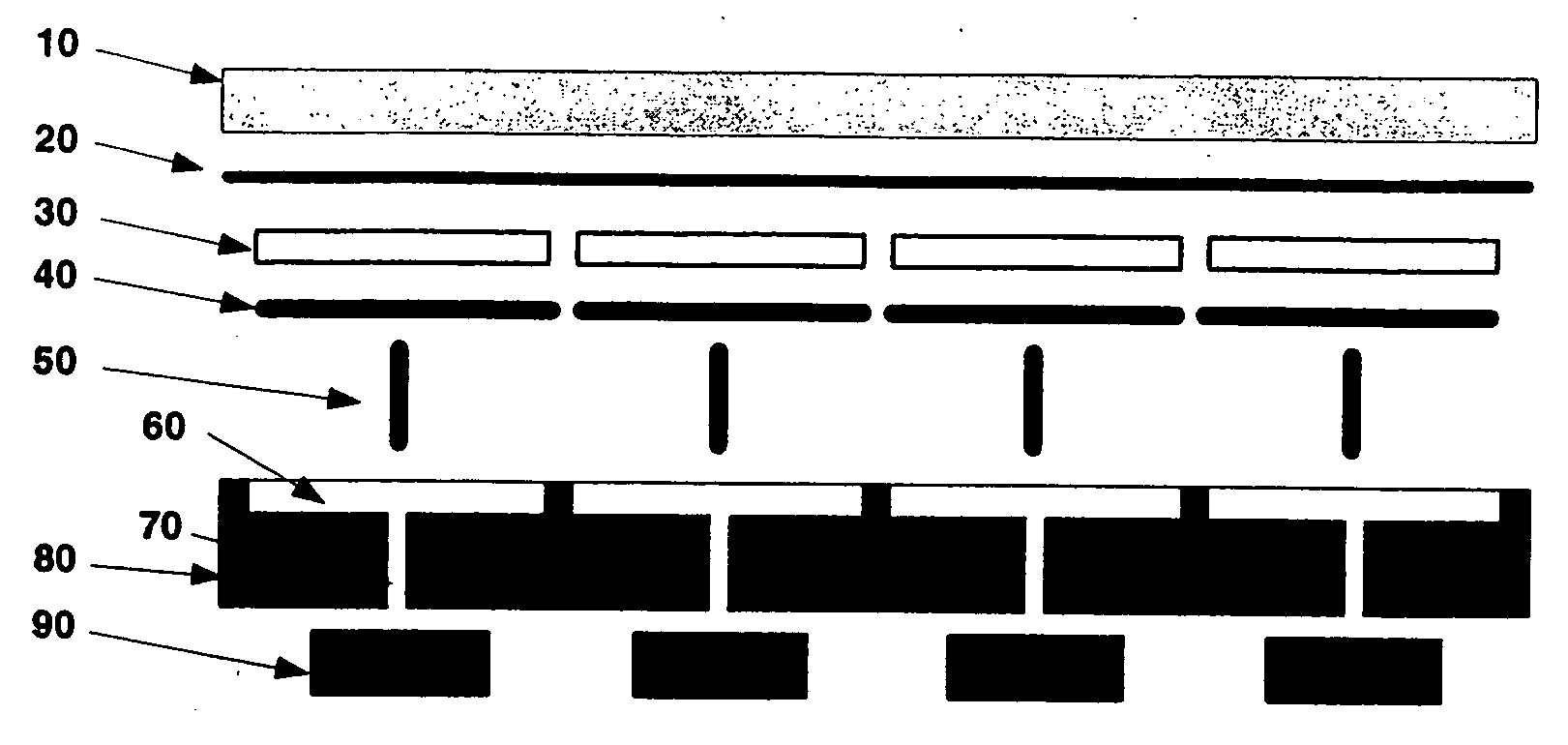
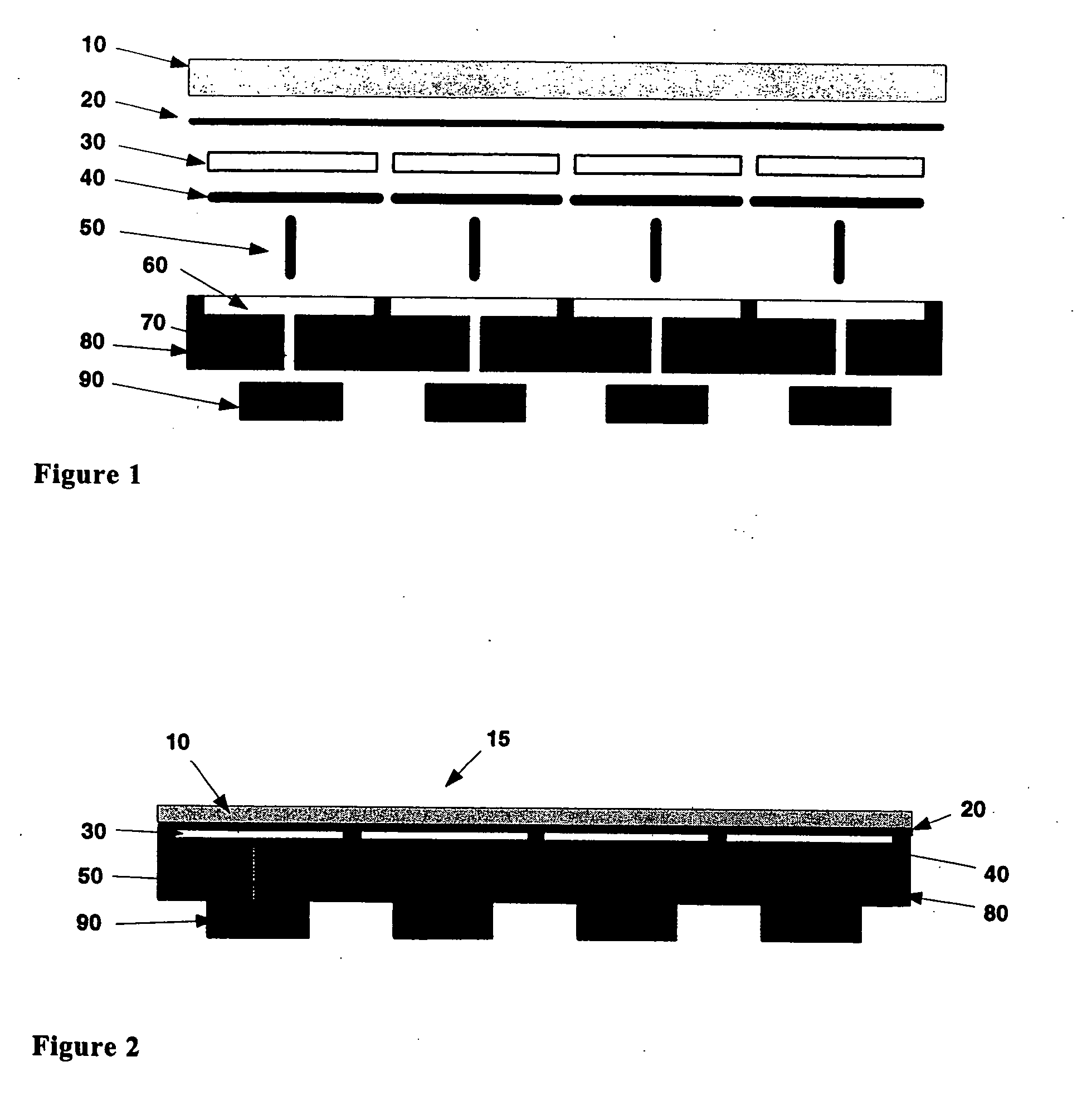
[0025]FIG. 1 shows a cross-section of the different components making the display.

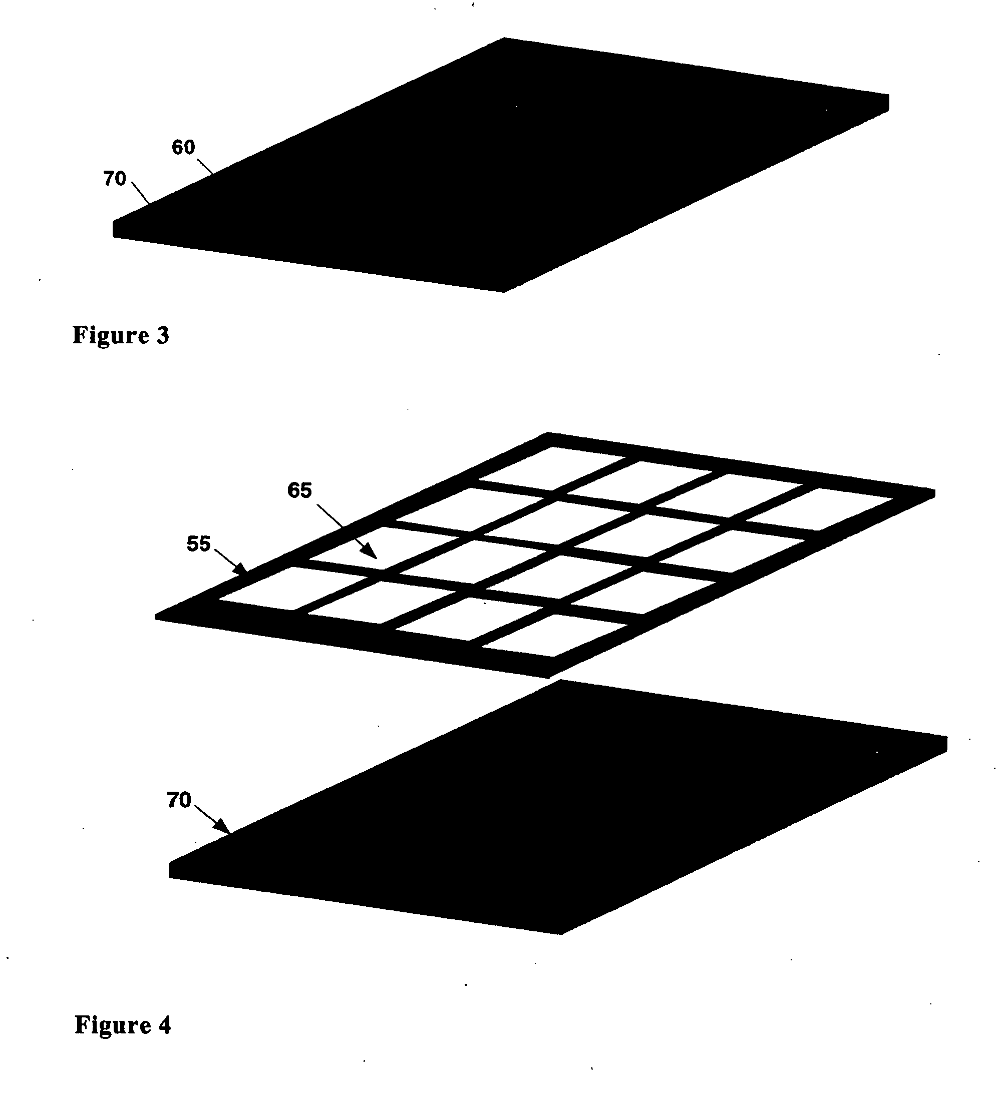
[0026] The base of the display is made of an isolating substrate 80 with small cavities 60 imprinted. These cavities 60 will make the picture elements or pixels of the assembled display. For further reference the cavities are referred to as micro pockets. The isolating substrate 80 can be made of a glassfibre composite, plastic, ceramics or another material with isolating characteristics. The micro pockets 60 may be formed by stamping, imprinting, engraving or etching in the substrate 80. After the micro pockets 60 are established, holes 70 in the centre of each micro pocket 60 are made. These holes 70 will in turn provide for an electrical connection between the underside of the substrate and each pocket 60. This connection will be established when a conductive material 40, 50 is applied t...


PUM

PropertyMeasurementUnit
transparent conductiveaaaaaaaaaa
transparentaaaaaaaaaa
conductiveaaaaaaaaaa

Abstract

The present invention relates to a thin display, and a method of manufacturing the same. The display comprises an isolated substrate, with cavities also called micro pockets in a pattern, or created with a separate sheet with holes mounted on the substrate. These micro pockets will make the picture elements of the display. The display further comprises perforated holes in the centre of the micro pockets and a conductive material covering the surfaces inside the micro pockets and the perforated holes. An electro-optical material fill the cavities, and a uniform layer of transparent conductive material cover all the filled micro pockets. A top layer of a transparent substrate cover the conductive layer.

Description

[0001] This application is a divisional application co-pending U.S. patent application Ser. No. 10 / 294,330, filed Nov. 14, 2002, which claims priority to U.S. Provisional Application No. 60 / 331,326 which was filed on Nov. 14, 2001, the entire disclosures of which are hereby incorporated by reference.FIELD OF INVENTION [0002] The present invention relates to a display, and a method of manufacturing the same. The display comprises an electrode layer, a substrate, which on the surface facing the electrode layer is covered with a set of electrode elements placed in cavities, and a layer of electro-optic material which is arranged between the electrode layer and the substrate. BACKGROUND OF THE INVENTION [0003] The present invention relates to the technical field of flat displays. An example of a display or screen according to that stated above (also called LCD, Liquid Crystal Display) is disclosed in SE-511,511 with the title: Display, relates to a liquid crystal display, comprising an ...

Claims


Application Information

Patent Timeline
Patent Type & Authority Applications(United States)
IPC IPC(8): G02F1/1333G02F1/1345G02F1/153G02F1/155H01L27/32H01L51/52
CPCG02F1/133377G02F1/1345G02F1/1533H01L2251/5315G02F2201/42H01L27/32H01L51/52G02F1/155Y10T442/259H10K2102/3026H10K59/80H10K50/80H10K59/00
Inventor HOLTER, BORRE
Owner POLYDISPLAY AS
Why Eureka
Try Eureka