MOSFET structures with conductive niobium oxide gates
a conductive niobium oxide and mosfet technology, applied in the direction of basic electric elements, electrical apparatus, semiconductor devices, etc., can solve the problems of high reactive nmos metals, unstable contact with gate dielectrics, and difficult processing of qualified nmos gate candidates, etc., to achieve the effect of low work function, low resistance and high resistan
- Summary
- Abstract
- Description
- Claims
- Application Information
AI Technical Summary
Benefits of technology
Problems solved by technology
Method used
Image

Examples
example 1
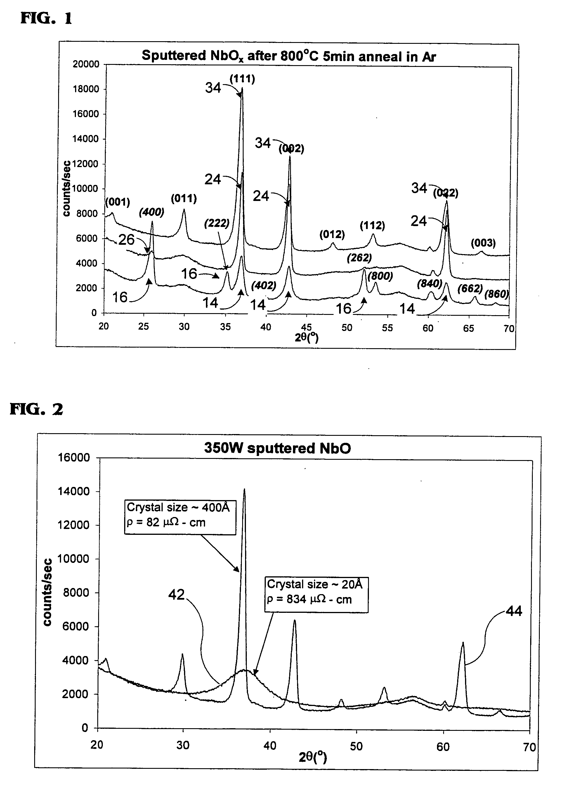
[0021] A 300 W sputtering power was used with an O2 partial pressure of approximately 30%. The O2 partial pressure was established using mass flow controllers to control the amount of both O2 and argon entering the sputtering chamber. The resulting film is a mix of NbO and NbO2, which corresponds to XRD plot 12 in FIG. 1. The NbO peaks 14 indicate the presence of NbO, while the NbO2 peaks 16 indicate the presence of NbO2. The results of this example may not contain a sufficient amount of NbO to act as a suitable gate material, but the example is presented to illustrate the effect of changing oxygen partial pressure.
example 2
[0022] A 300 W sputtering power was used with an O2 partial pressure of approximately 25%. The O2 partial pressure was established using mass flow controllers to control the amount both O2 and argon entering the sputtering chamber. The resulting film, which corresponds to XRD plot 22, is predominantly NbO, with detectable levels of NbO2. An NbO2 peak 26 is still discernable, but the NbO peaks 24 are even more apparent than in Example 1. Although, some NbO2 is present this predominantly NbO film is suitable for use as an NbO gate.
example 3
[0023] The sputtering power was increased to 350 W while the O2 partial pressure was maintained at approximately 25%. The O2 partial pressure was established using mass flow controllers to control the amount both O2 and argon entering the sputtering chamber. The resulting film, which corresponds to XRD plot 32, is predominantly NbO, without any discernable NbO2 peaks. The NbO peaks 34 are even more apparent than in Example 2.
[0024] Among the three examples just provided, Example 3 provides a NbO film with the least amount of discernable NbO2. Example 2 may still be suitable for use as an NbO gate, provided the increased resistivity caused by the NbO2 does not significantly degrade the overall performance as an NMOS gate.
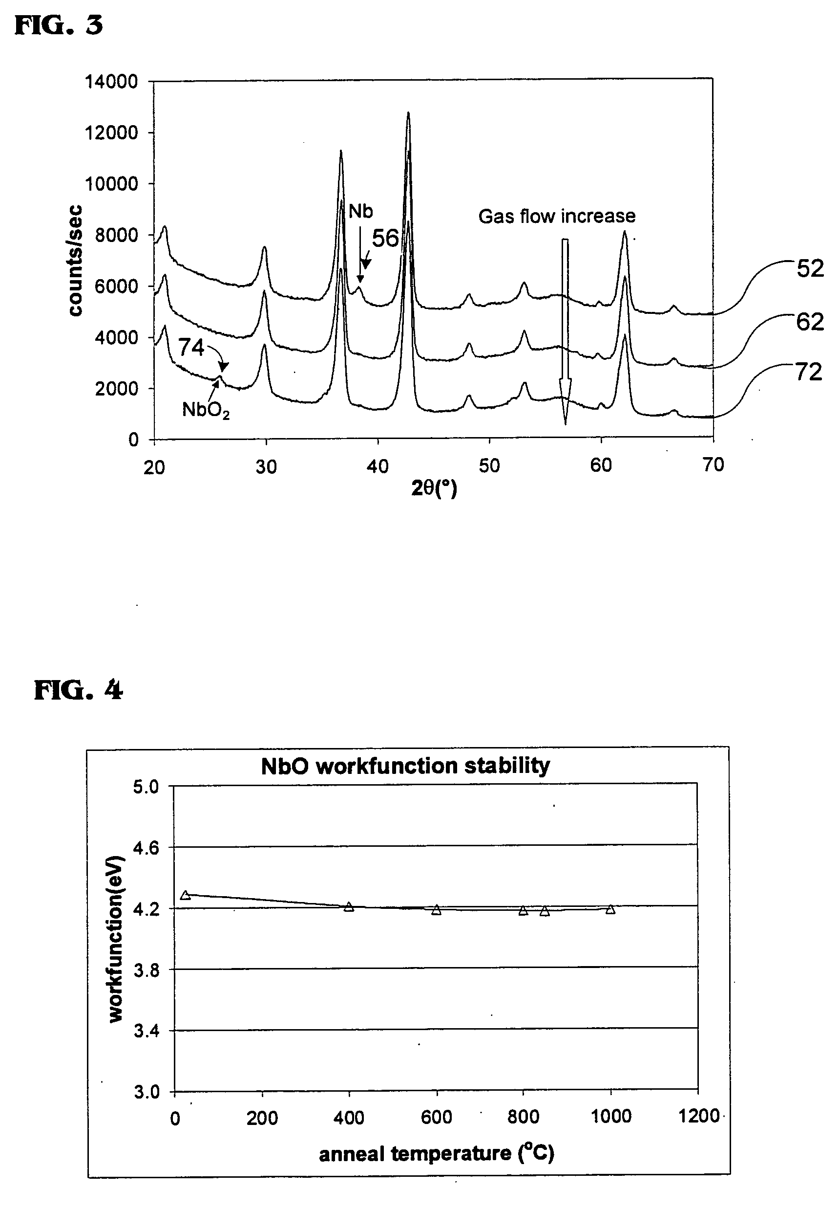
[0025]FIG. 2 shows XRD measurements for the material produced by Example 3, before and after anneal at approximately 800 degrees Celsius for approximately 5 minutes in argon. FIG. 2 shows that the as-deposited NbO film, which corresponds to XRD plot 42, has a broad...
PUM
 Abstract
Description
Claims
Application Information
 - R&D
- Intellectual Property
- Life Sciences
- Materials
- Tech Scout
- Unparalleled Data Quality
- Higher Quality Content
- 60% Fewer Hallucinations
Browse by: Latest US Patents, China's latest patents, Technical Efficacy Thesaurus, Application Domain, Technology Topic, Popular Technical Reports.
© 2025 PatSnap. All rights reserved.Legal|Privacy policy|Modern Slavery Act Transparency Statement|Sitemap|About US| Contact US: help@patsnap.com