


Quick Research
Generate reliable direction feasibility study reports for your R&D in just a few steps.

Technical Q&A
Discover and master advanced knowledge NOW. Basics, ideas, possibilities, all at once.

Find Solutions
As an expert in R&D theories, this can generate solutions to your technical problems instantly.

Evaluate Feasibility
Analyze your overall solution with one click, know your potential R&D risks in advance.

Monitor Landscape
Get weekly tech updates, stay abreast of the latest tech innovations and key insights.
Spinel boules, wafers, and methods for fabricating same
a technology of spinel boules and wafers, applied in the field of spinel boules, wafers and methods for fabricating same, can solve the problems of reducing throughput, low yield, and numerous drawbacks of spinel boules
- Summary
- Abstract
- Description
- Claims
- Application Information
AI Technical Summary
Problems solved by technology
Method used
Image

Examples
example
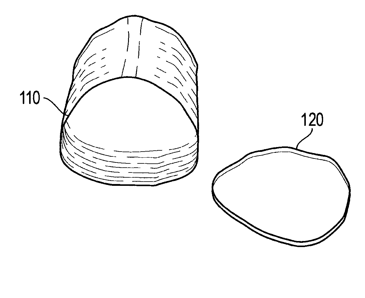
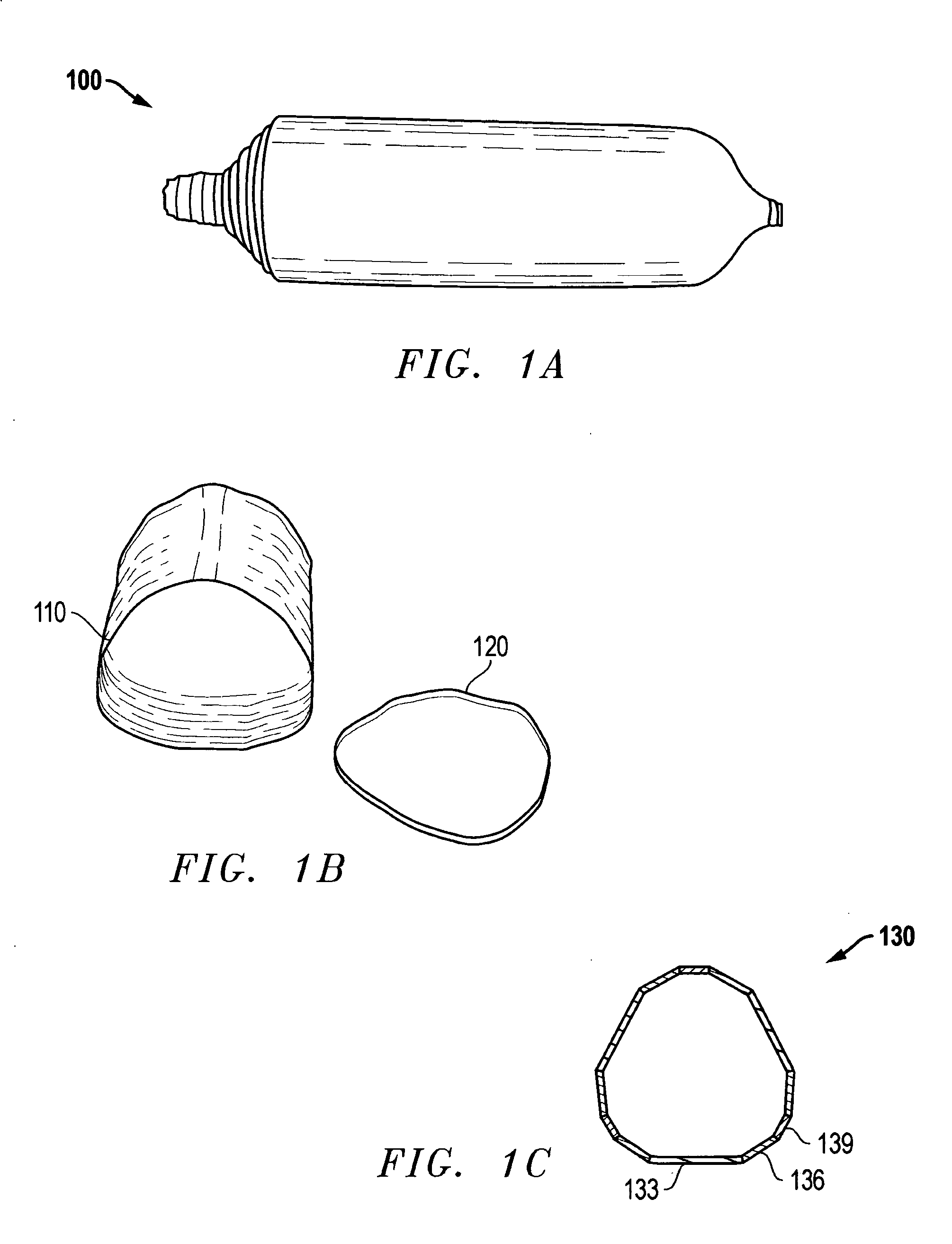
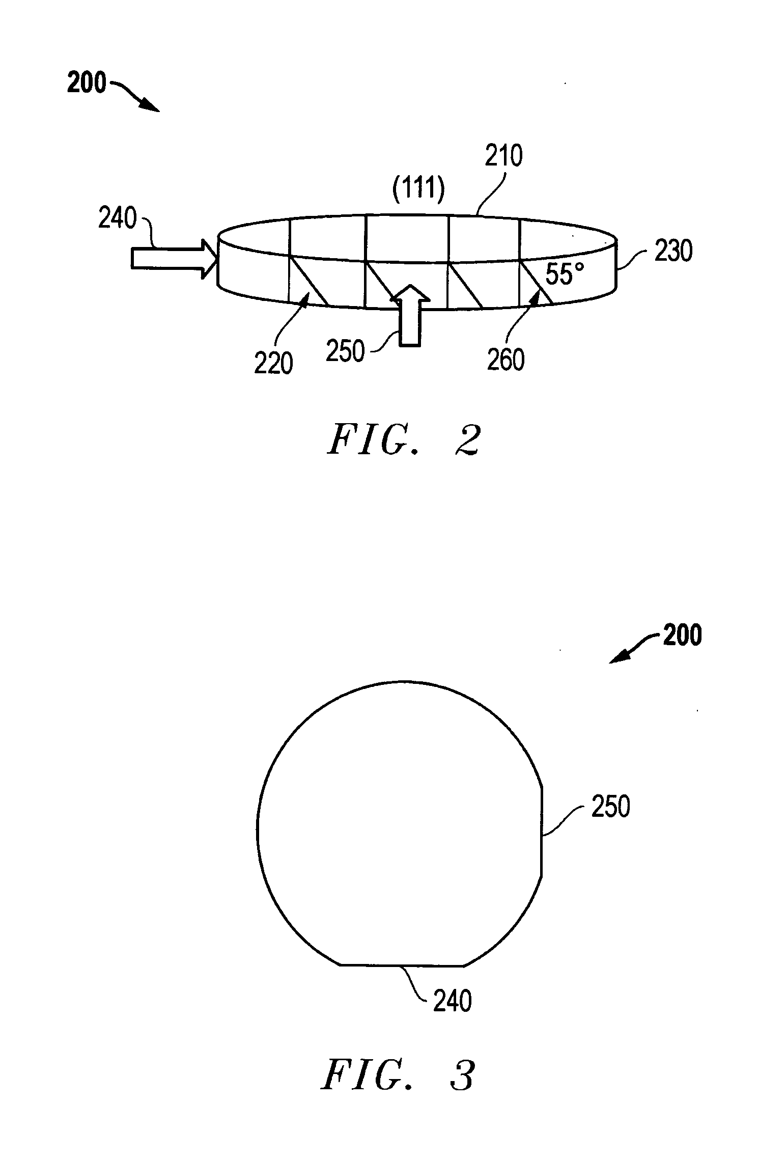
[0042] A boule (ingot) grown by the Czochralski technique had the top and tail removed to produce two flat surfaces. The boule ends (the two flat surfaces) were x-rayed using a Laue backscattered technique to verify orientation and to identify 1) the front-side for future wafers to ensure the (100) cleavage plane will cleave from the bottom face of the future wafers to the top face with the intersection line on the bottom being further from the to-be formed major flat than the intersection line on the top and 2) the approximate position of the major (1-1-2) (or (2-2-4)) and minor (01-1) (or (02-2)) flats. The boule ends were then x-rayed to measure the orientation and to align the axis of the boule to the direction.
[0043] The boule was then turned to a diameter of approximately 2″ to form a cylinder exactly parallel to the 111 direction (that is, the central axis was parallel to the orientation). At this point the major and minor flat directions were marked on the top face by scr...
PUM
| Property | Measurement | Unit |
|---|---|---|
| Angle | aaaaa | aaaaa |
| Angle | aaaaa | aaaaa |
| Angle | aaaaa | aaaaa |
Abstract
Description
Claims
Application Information
 - R&D Engineer
- R&D Manager
- IP Professional
- Industry Leading Data Capabilities
- Powerful AI technology
- Patent DNA Extraction
Browse by: Latest US Patents, China's latest patents, Technical Efficacy Thesaurus, Application Domain, Technology Topic, Popular Technical Reports.
© 2024 PatSnap. All rights reserved.Legal|Privacy policy|Modern Slavery Act Transparency Statement|Sitemap|About US| Contact US: help@patsnap.com