
Solid-state image pickup device

a solid-state image and pickup device technology, applied in the field of solid-state image pickup devices, can solve the problems of reducing the gain of the source follower circuit, affecting the conversion efficiency and affecting the so as to reduce the power consumption of the solid-state image pickup device without deteriorating the conversion efficiency or frequency characteristic of the signal

Inactive Publication Date: 2005-03-03
SONY CORP
View PDF9 Cites 5 Cited by
  • Summary
  • Abstract
  • Description
  • Claims
  • Application Information

AI Technical Summary

Benefits of technology

The present invention has been accomplished in view of the problems mentioned above. And it is an object of the invention to provide a solid-state image pickup device adapted to realize a reduction of the power consumption without deteriorating the conversion efficiency or the frequency characteristic thereof.
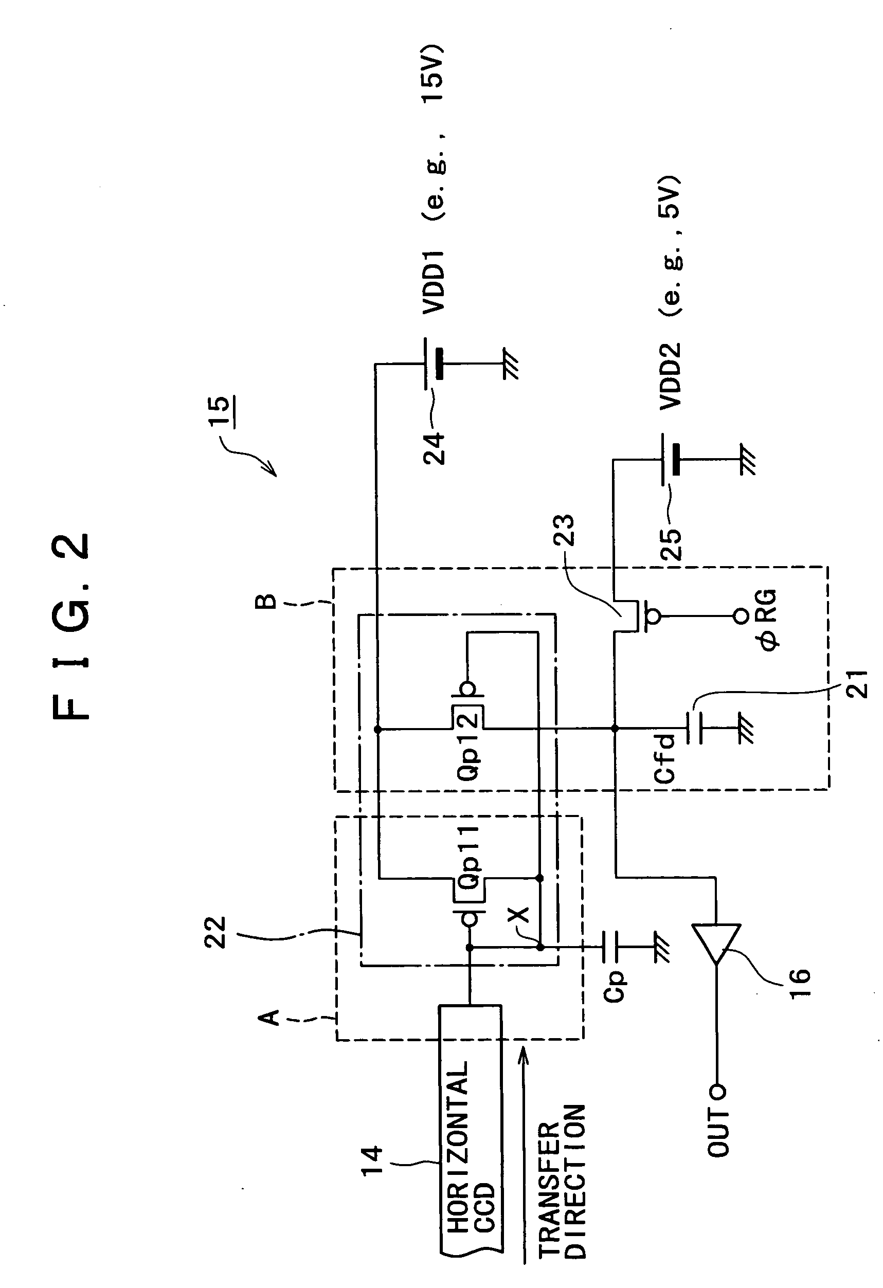
Thus, according to the present invention, the reset voltage for the floating diffusion region is settable independently of the potential of the charge transferrer, so that the reset voltage for the floating diffusion region can be lowered to consequently reduce the power consumption in the solid-state image pickup device without deteriorating the conversion efficiency or the frequency characteristic thereof.

Problems solved by technology

As a result, there arises a problem that the gain of the source follower circuit is lowered due to the substrate bias effect to eventually deteriorate the sensitivity.
However, since it is difficult to produce a depletion-mode Pch MOS transistor whose threshold voltage Vth is 4 V or so, the output voltage value needs to be lowered from 15 V or so to 3 V or so in the first-stage and second-stage source follower circuits.
For this purpose, the gate-source voltage Vgs in each of the first-stage and second-stage source follower circuit needs to be set to 6 V or so, hence raising another problem that the gain of each source follower circuit is further impaired due to the substrate bias effect.

Method used


Image

  • Solid-state image pickup device
  • Solid-state image pickup device
  • Solid-state image pickup device

Examples


Embodiment Construction

Hereinafter some preferred embodiments of the present invention will be described in detail with reference to the accompanying drawings. In the embodiments, an explanation will be given on an exemplary case of applying the invention to a solid-state image pickup device which adopts an interline transfer system, for example. However, the present invention is not limited thereto alone, and it may be applied also to any solid-state image pickup device adopting some other transfer system such as a frame interline transfer system.

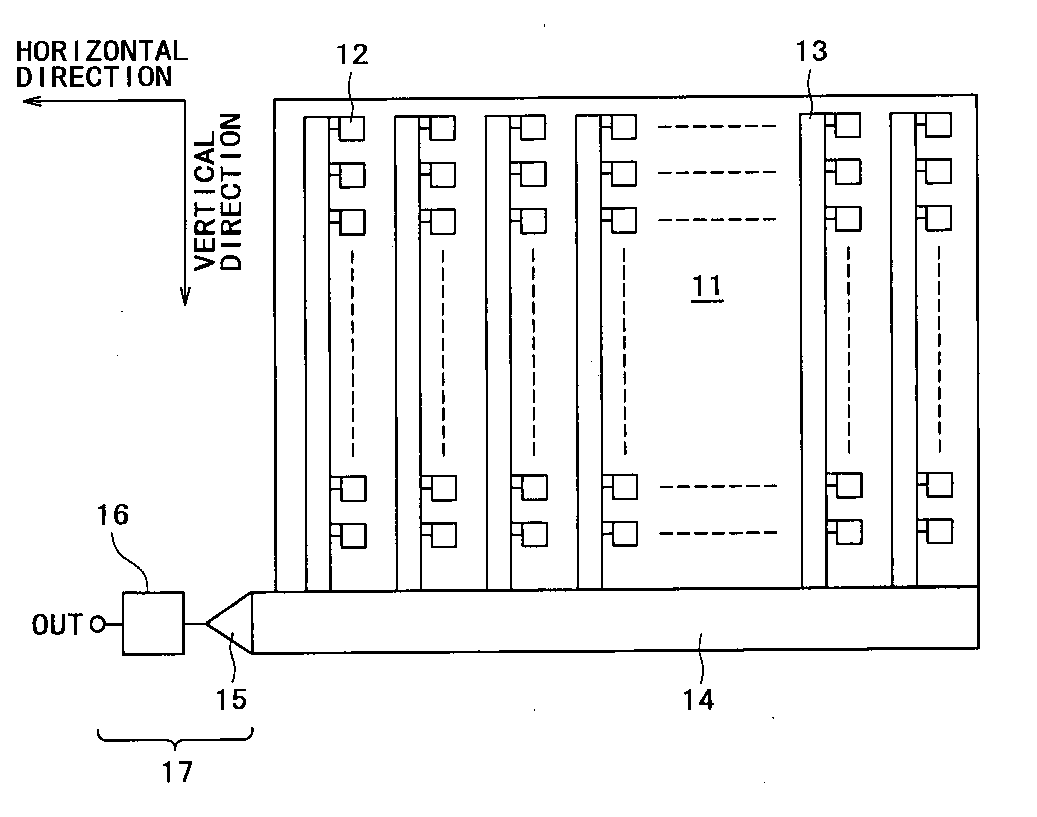
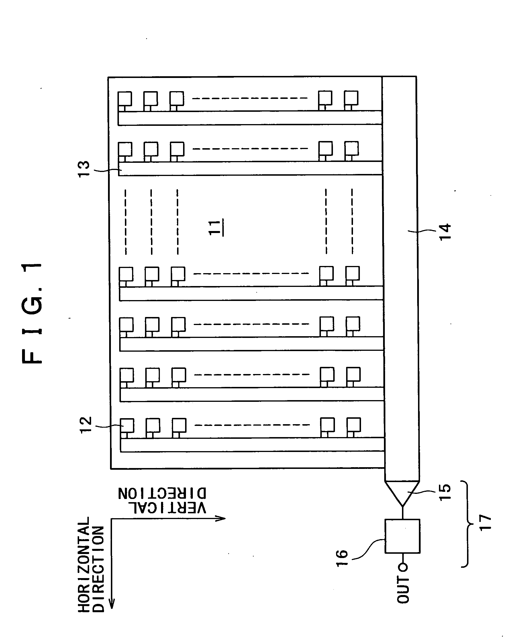
FIG. 1 is a block diagram schematically showing the whole structure of a solid-state image pickup device, e.g., a CCD (Charge Coupled Device) type solid-state image pickup device according to an embodiment of the present invention. In FIG. 1, a charge detector 15 and an output buffer 16 constituting an output circuit 17 are formed integrally, in combination with an image sensor 11 and a horizontal CCD (horizontal transferrer) 14, on an N-type semiconductor sub...


PUM


Abstract

A solid-state image pickup device including a charge transferrer to transfer a signal charge obtained through photoelectric conversion; a floating diffusion region; a reset means for resetting the potential of the floating diffusion region; and a current source for supplying, to the floating diffusion region, a signal charge corresponding to the quantity of the signal charge transferred by the charge transferrer. The current source such as a current mirror circuit is interposed between the output stage of a horizontal CCD and the floating diffusion region so as to supply thereto a signal charge corresponding to the quantity of the signal charge transferred by the horizontal CCD, hence separating the horizontal CCD and the floating diffusion region potentially from each other, whereby the supply voltage, i.e., the reset voltage for the floating diffusion region, can be set independently of the potential of the horizontal CCD.

Description

BACKGROUND OF THE INVENTION The present invention relates to a solid-state image pickup device, and more particularly to an output circuit of a solid-state image pickup device wherein a signal charge obtained in each light receiving element through photoelectric conversion is transferred by a charge transferrer and then is outputted after conversion into a corresponding signal voltage. It is known that, for the purpose of reducing the power consumption in a solid-state image pickup device, an output buffer in an output circuit to convert a signal charge into a corresponding signal voltage and to output the same therefrom includes plural cascade-connected stages of source follower circuits, wherein respective supply voltages to the source follower circuits are set to be mutually different, in such a manner that the greater the DC current flowing in each source follower circuit, the lower the supply voltage to each of the plural stages of the source follower circuits (see Cited Pate...

Claims


Application Information

Patent Timeline
IPC IPC(8): H01L27/148H01L27/14H01L31/10H04N5/335H04N5/372
CPCH04N5/378H04N25/75H04N3/1568H01L27/148
Inventor HARADA, KOUICHI
Owner SONY CORP
Learn More