Method of fabricating display device
a display device and a technology of a display device, applied in the field of fabricating a display device, can solve the problems of increasing the thickness of the leveling film, and achieve the effects of reducing the aperture ratio, avoiding the loss of light shielding pattern, and improving reflectan
- Summary
- Abstract
- Description
- Claims
- Application Information
AI Technical Summary
Benefits of technology
Problems solved by technology
Method used
Image
Examples
embodiment 1
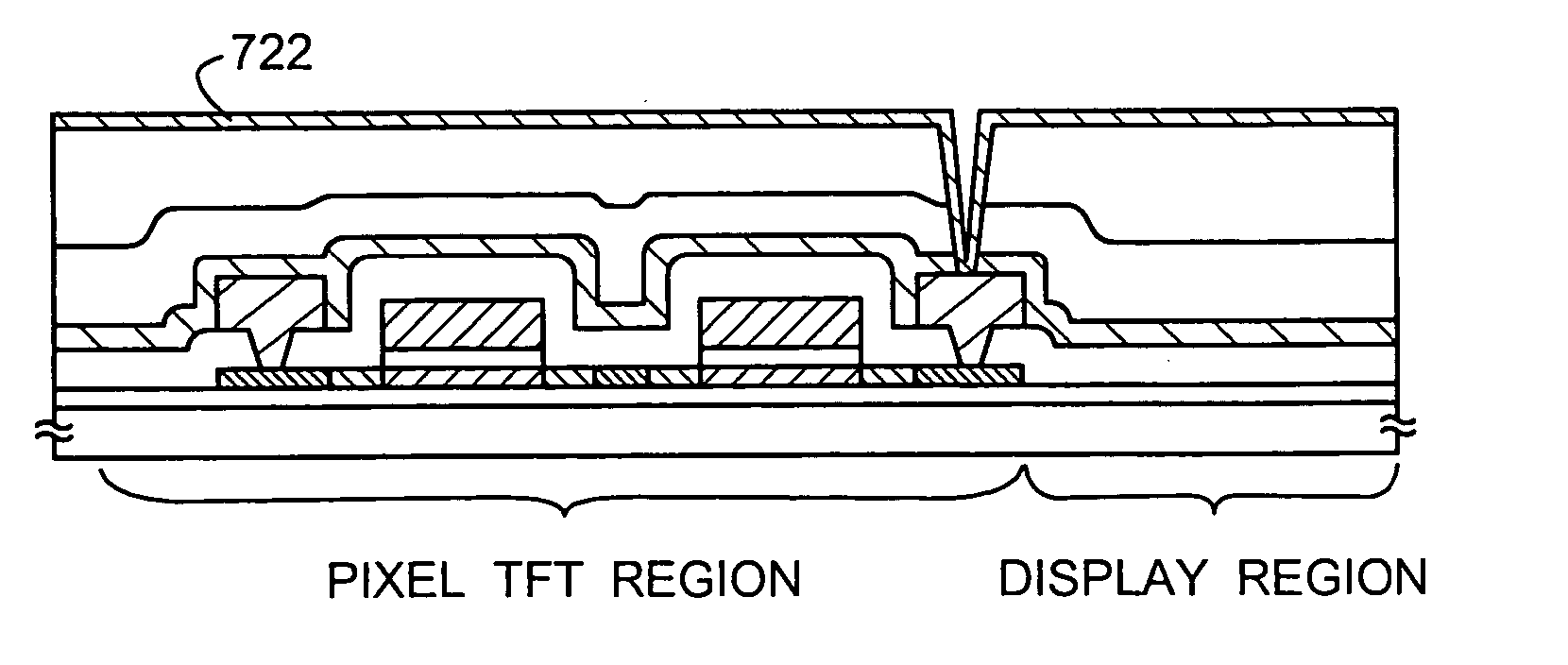
Embodiment 1 of the present invention will be described with reference to FIGS. 7A to 9C. A method of fabricating an active matrix substrate, particularly a pixel portion, will be herein described. The pixel portion includes a pixel TFT region that is a TFT provided in a pixel and a display region that does not include the TFT region.
In FIG. 7A, a glass substrate or a quartz substrate can be used as a substrate 700. A silicon substrate, a metal substrate or a stainless substrate on which an insulating film is formed may also be used for the substrate 700. A plastic substrate having a sufficient heat resistance can also be used.
Then, on the surface of the substrate 700 where a TFT is to be formed, a base film 701 made of an insulating film containing silicon is formed. In this embodiment, a silicon nitride oxide film having a thickness of 200 nm is formed as the base film 701.
Successively, an amorphous semiconductor film (in this embodiment, an amorphous silicon film) 702 havi...
embodiment 2
In Embodiment 2, the case where a pixel TFT having a different structure from that of Embodiment 1 is to be fabricated will be described. Since only a part of fabrication steps are different from those of Embodiment 1, the same fabrication steps are designated by the same reference numerals.
In accordance with the process of Embodiment 1, the fabrication steps up to the formation of the passivation film 718 are conducted. The first leveling film 719 is formed to a thickness of 0.3 μm (FIG. 9A). Then, the second leveling film 720 is formed to a thickness of 1.2 μm on the first leveling film 719. As the first leveling film 719 and the second leveling film 720, a polyimide resin, an acrylic resin, a resin containing a siloxane structure or an inorganic SOG material can he used. In this embodiment, an acrylic resin is used.
Since the first leveling film 719 has a thickness of 0.3 μm and the second leveling film 720 has a thickness of 1.2 μm, the total thickness of the films as the se...
embodiment 3
In this embodiment, the steps for fabricating an active matrix liquid crystal display device using the active matrix substrate fabricated in Embodiment 1 or Embodiment 2 will be described. As shown in FIG. 10, an orientation film 1001 is formed on the substrate in the state shown in FIG. 9C. A polyimide film is used as the orientation film in this embodiment. For a counter substrate 1002, a counter electrode 1003 and an orientation film 1004 are formed. A color filter or a shielding film may be formed on the counter substrate as needed.
Next, after formation of the orientation films, a rubbing treatment is performed so as to orient liquid crystal molecules at a certain pretilt angle. Then, the active matrix substrate on which the pixel portion and driving circuits are formed is bonded with the counter substrate by a known cell assembling step through a sealing material or a spacer (not shown). Thereafter, liquid crystal 1005 is injected into a gap between the substrates and is the...
PUM
| Property | Measurement | Unit |
|---|---|---|
| thickness | aaaaa | aaaaa |
| thickness | aaaaa | aaaaa |
| thickness | aaaaa | aaaaa |
Abstract
Description
Claims
Application Information
 - R&D
- Intellectual Property
- Life Sciences
- Materials
- Tech Scout
- Unparalleled Data Quality
- Higher Quality Content
- 60% Fewer Hallucinations
Browse by: Latest US Patents, China's latest patents, Technical Efficacy Thesaurus, Application Domain, Technology Topic, Popular Technical Reports.
© 2025 PatSnap. All rights reserved.Legal|Privacy policy|Modern Slavery Act Transparency Statement|Sitemap|About US| Contact US: help@patsnap.com


