Position modulated optical reflectance measurement system for semiconductor metrology

a technology of optical reflectance and measurement system, applied in the field of optical methods, can solve the problems of difficult control of these two processes, and changes in optical reflectivity at the sample surfa

Inactive Publication Date: 2005-02-17
THERMA WAVE INC
View PDF11 Cites 34 Cited by
  • Summary
  • Abstract
  • Description
  • Claims
  • Application Information

AI Technical Summary

Problems solved by technology

Correctly controlling these two processes may be difficult, especially in the ultra-shallow junction case, where the implanted layer is very thin and highly doped.
In turn, this results in changes in the optical reflectivity at the sample surface.

Method used


Image

  • Position modulated optical reflectance measurement system for semiconductor metrology
  • Position modulated optical reflectance measurement system for semiconductor metrology
  • Position modulated optical reflectance measurement system for semiconductor metrology

Examples


Embodiment Construction

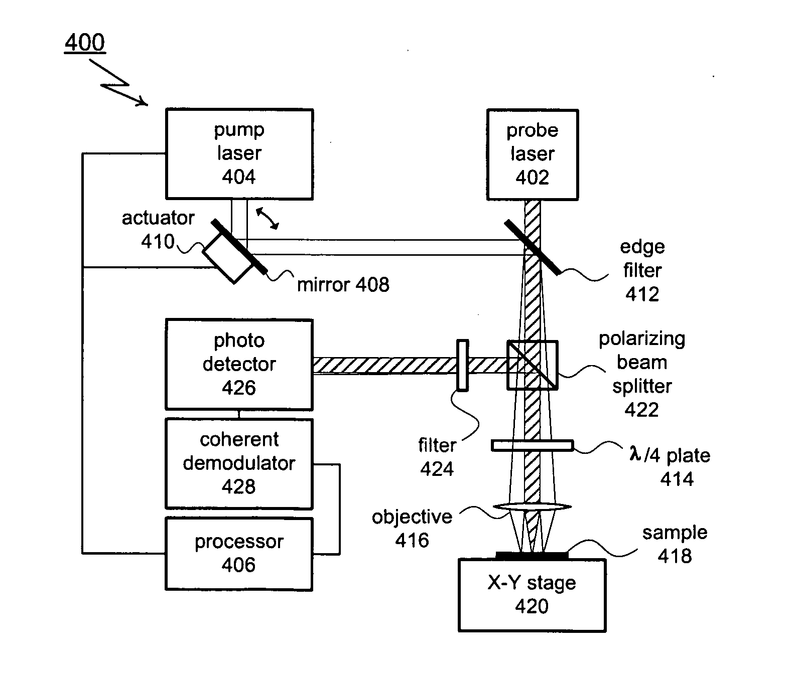
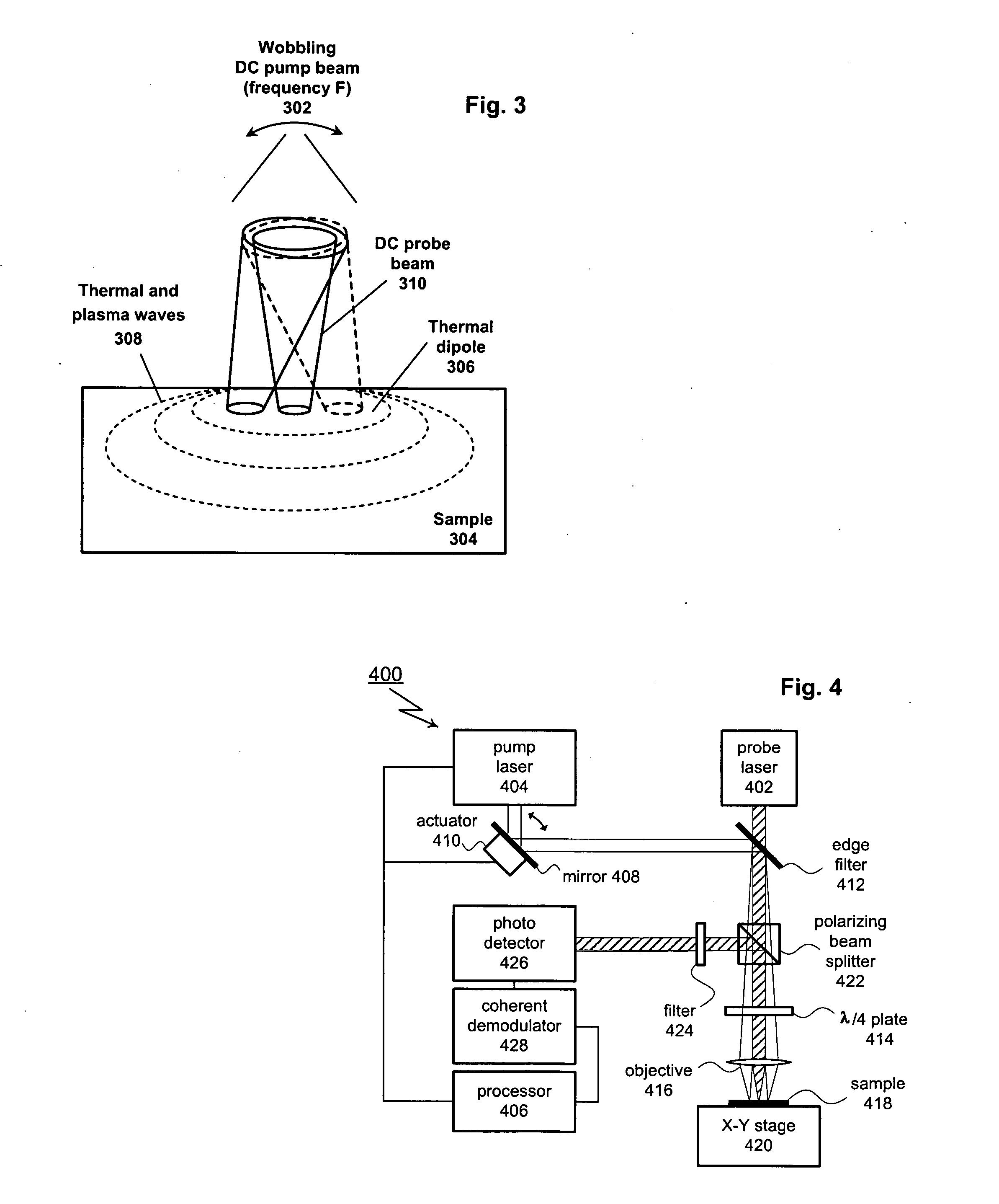
[0020] An embodiment of the present invention includes a method and apparatus for photo modulated optical response (MOR)-based evaluation of semiconductor samples in which a position modulated pump beam is used in place of conventional intensity-modulated techniques. As shown in FIG. 3, the basic technique uses a DC (constant intensity) pump beam 302 that is focused on the surface of a sample being analyzed 304. The position of the illumination spot produced by the pump beam 302 is modulated or scanned back and forth over the surface of the sample. Optical absorption of the pump irradiation creates a spatially elongated region close to the sample surface that acts as a thermal dipole 306. The lateral dimension of this elongated region may be up to several probe and / or pump beam diameters.

[0021] Thermal and plasma waves 308 propagate from the thermal dipole 306 creating region of modulated optical reflectance. Due to a specific geometry of the localized heat source on the semiconduc...


PUM

PropertyMeasurementUnit
wavelengthaaaaaaaaaa
optical reflectanceaaaaaaaaaa
areaaaaaaaaaaa

Abstract

A system for evaluating semiconductor wafers includes illumination sources for generating probe and pump beams. The pump beam is focused on the surface of a sample and a beam steering mechanism is used to modulate the point of focus in a predetermined pattern. The moving pump beam introduces thermal and plasma waves in the sample causing changes in the reflectivity of the surface of the sample. The probe beam is focused within or adjacent to the area illuminated by the pump beam. The reflected probe beam is gathered and used to measure the changes in reflectivity induced by the pump beam. By analyzing changes in reflectivity, a processor is able to deduce structure and chemical details of the sample.

Description

PRIORITY CLAIM [0001] The present application claims priority to U.S. Provisional Patent Application Ser. No. 60 / 495,195, filed Aug. 14, 2003, the disclosure of which is incorporated in this document by reference.TECHNICAL FIELD [0002] The subject invention relates generally to optical methods for inspecting and analyzing semiconductor wafers and other samples. In particular, the subject invention relates to methods for characterizing the effectiveness of implantation and annealing processes for samples both with and without ultra-shallow junctions. BACKGROUND OF THE INVENTION [0003] Ion implantation and annealing are two processes used during the fabrication of integrated circuits. Ion implantation introduces charged atoms (ions) into the surface region of a semiconductor wafer. Annealing removes damage (changes to the crystalline lattice) that occurs as a side effect of the implantation process. The annealing process also activates implanted ions and changes the type of electrical...

Claims


Application Information

Patent Timeline
Patent Type & Authority Applications(United States)
IPC IPC(8): G01N21/63
CPCG01N21/636G01N21/1717G01N21/9501G01N21/9505
Inventor OPSAL, JONNICOLAIDES, LENASALNIK, ALEX
Owner THERMA WAVE INC
Why Eureka
Try Eureka