Photocurrent-to-voltage conversion apparatus including non-diode-connected clamping MOS transistor
a technology of photocurrent and voltage conversion, which is applied in the direction of pulse generators, pulse techniques, instruments, etc., can solve the problems of waveform distortion between photocurrent and detection voltage, inaccurate light transmission, and still generation of detection voltage, so as to suppress the saturation of an operational amplifier
- Summary
- Abstract
- Description
- Claims
- Application Information
AI Technical Summary
Benefits of technology
Problems solved by technology
Method used
Image

Examples
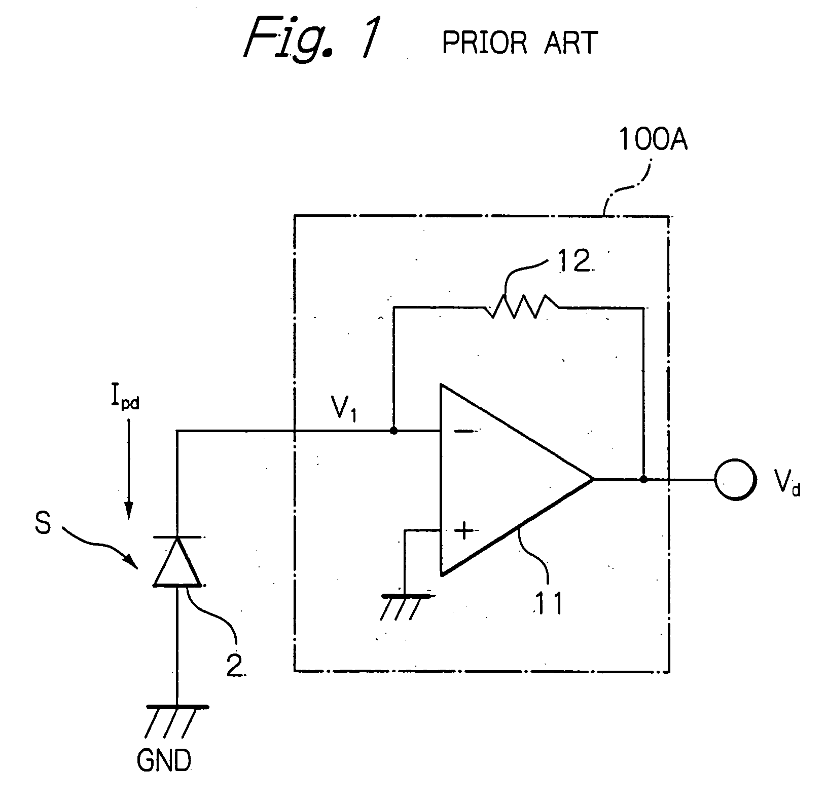
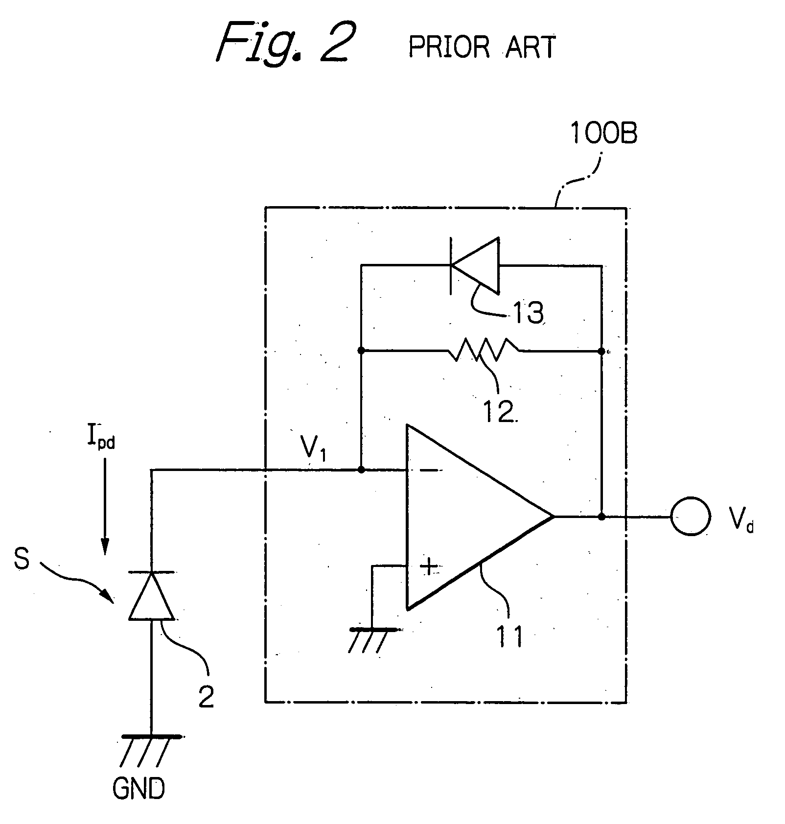
first embodiment
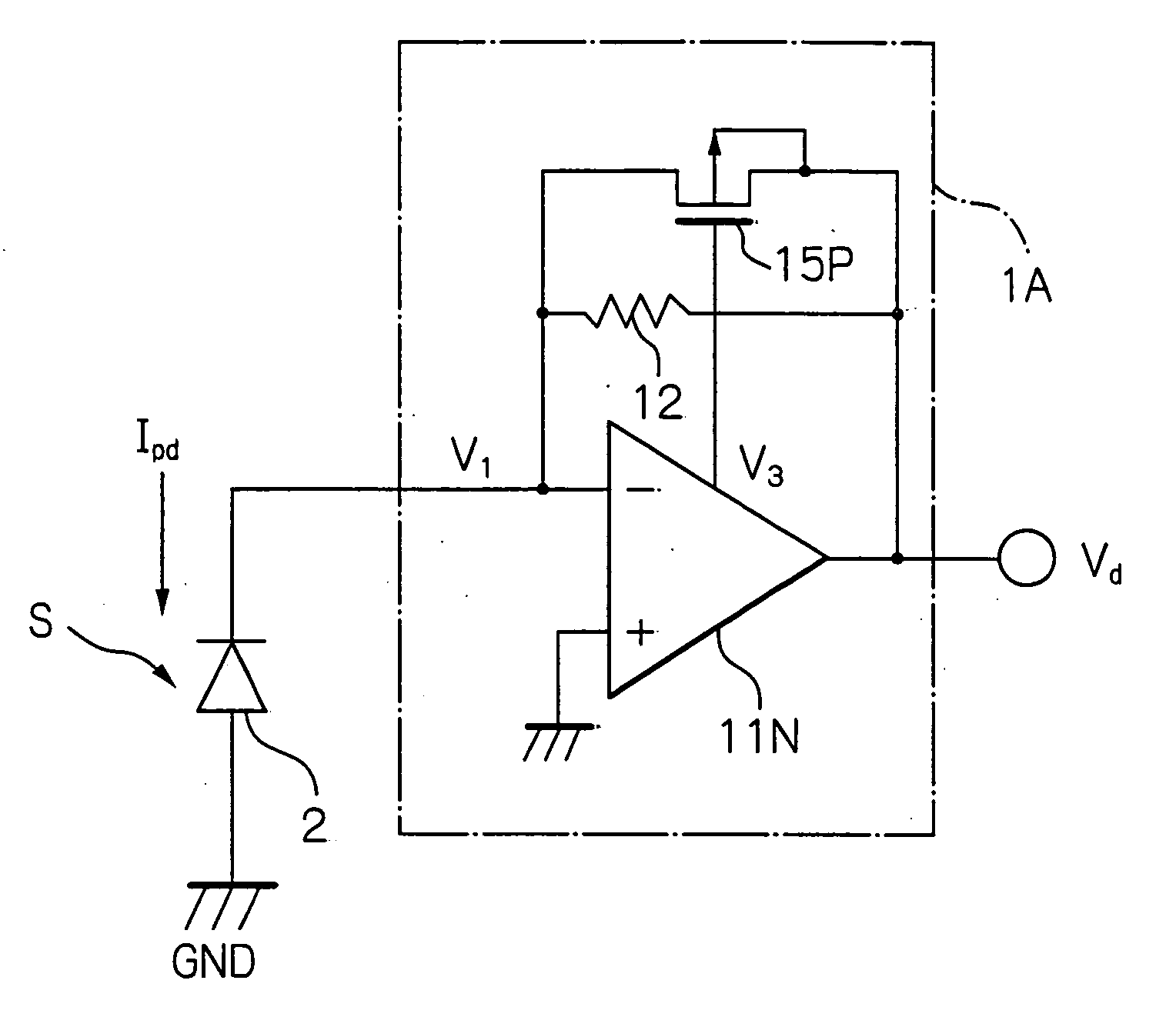
In FIG. 6A, which illustrates the photocurrent-to-voltage conversion apparatus according to the present invention, this photocurrent-to-voltage conversion apparatus 1A is constructed by a P-channel enhancement-type MOS transistor 15P instead of the N-channel enhancement-type MOS transistor 14N of FIG. 3. In this case, a clamp voltage VCL of the P-channel enhancement-type MOS transistor 15P is determined by the absolute value of a threshold voltage Vthp of the P-channel MOS transistor 15P. Also, the photocurrent-to-voltage conversion apparatus 1A is constructed by an operational amplifier 11N of an N-channel inverter type instead of the operational amplifier 11 of FIG. 3.
The P-channel enhancement-type MOS transistor 15P is non-diode-connected, i.e., the gate of the P-channel MOS transistor 15P is connected to an intermediate stage of the operational amplifier 11N.
As illustrated in FIG. 6B, the operational amplifier 11N is constructed by a plurality of inverter stages which are in ...
second embodiment
In FIG. 10A, which illustrates the photocurrent-to-voltage conversion apparatus according to the present invention, the gate voltage of the MOS transistor 15P of this photocurrent-to-voltage conversion apparatus 1C is derived from the output voltage V2 of the first inverter stage (111, 112N) as illustrated in FIG. 10B.
As shown in FIG. 11A, the photocurrent-to-voltage conversion apparatus 1C of FIG. 10A is effective when the saturated voltage of the operational amplifier 11N is large so that the saturated difference between the detection voltage Vd and the voltage V1 is larger than the clamp voltage VCL determined by the threshold voltage Vthp of the P-channel MOS transistor 15P.
The operation of the photocurrent-to-voltage conversion apparatus 1C of FIGS. 10A and 10B is explained next with reference to FIG. 11B.
First, before time t1, no photocurrent Ipd flows through the photodiode 2. As a result, since no current flows through the negative feedback resistor 12, the detection vo...
third embodiment
In FIG. 14A, which illustrates the photocurrent-to-voltage conversion apparatus according to the present invention, photocurrent-to-voltage conversion apparatus 1E includes an N-channel enhancement-type MOS transistor 15N instead of the P-channel enhancement-type MOS transistor 15P of FIG. 10A. The gate voltage of the N-channel enhancement-type MOS transistor 15N is also derived from the output voltage V2 of the first inverter stage (111, 112N) as illustrated in FIG. 14B.
As shown in FIG. 15A, the photocurrent-to-voltage conversion apparatus 1E of FIG. 14A is effective when the saturated voltage of the operational amplifier 11N is large so that the saturated difference between the detection voltage Vd and the voltage V1 is larger than a clamp voltage VCL determined by the threshold voltage Vthn of the N-channel MOS transistor 15N.
The operation of the photocurrent-to-voltage conversion apparatus 1E of FIGS. 14A and 14B is explained next with reference to FIG. 15B.
First, before ti...
PUM
 Abstract
Description
Claims
Application Information
 - R&D
- Intellectual Property
- Life Sciences
- Materials
- Tech Scout
- Unparalleled Data Quality
- Higher Quality Content
- 60% Fewer Hallucinations
Browse by: Latest US Patents, China's latest patents, Technical Efficacy Thesaurus, Application Domain, Technology Topic, Popular Technical Reports.
© 2025 PatSnap. All rights reserved.Legal|Privacy policy|Modern Slavery Act Transparency Statement|Sitemap|About US| Contact US: help@patsnap.com