
Integrated network-port socket and physical-layer device and main board incorporating the same

Inactive Publication Date: 2005-01-27
VIA TECH INC
View PDF4 Cites 11 Cited by
  • Summary
  • Abstract
  • Description
  • Claims
  • Application Information

AI Technical Summary

Benefits of technology

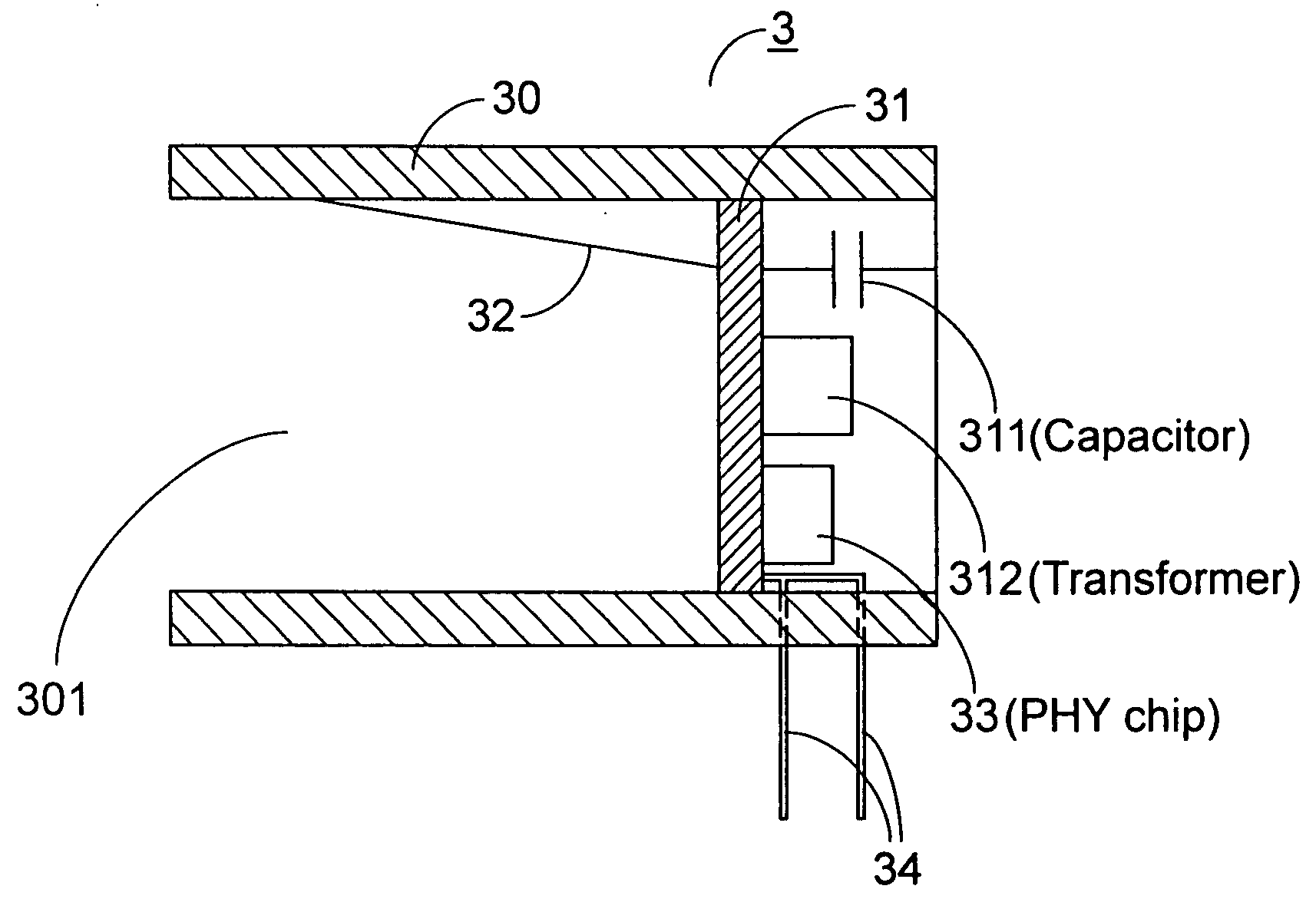
[0003] The present invention provides a network-port socket structure, which is close to the PHY chip so as to minimize the return loss and insertion loss.

Problems solved by technology

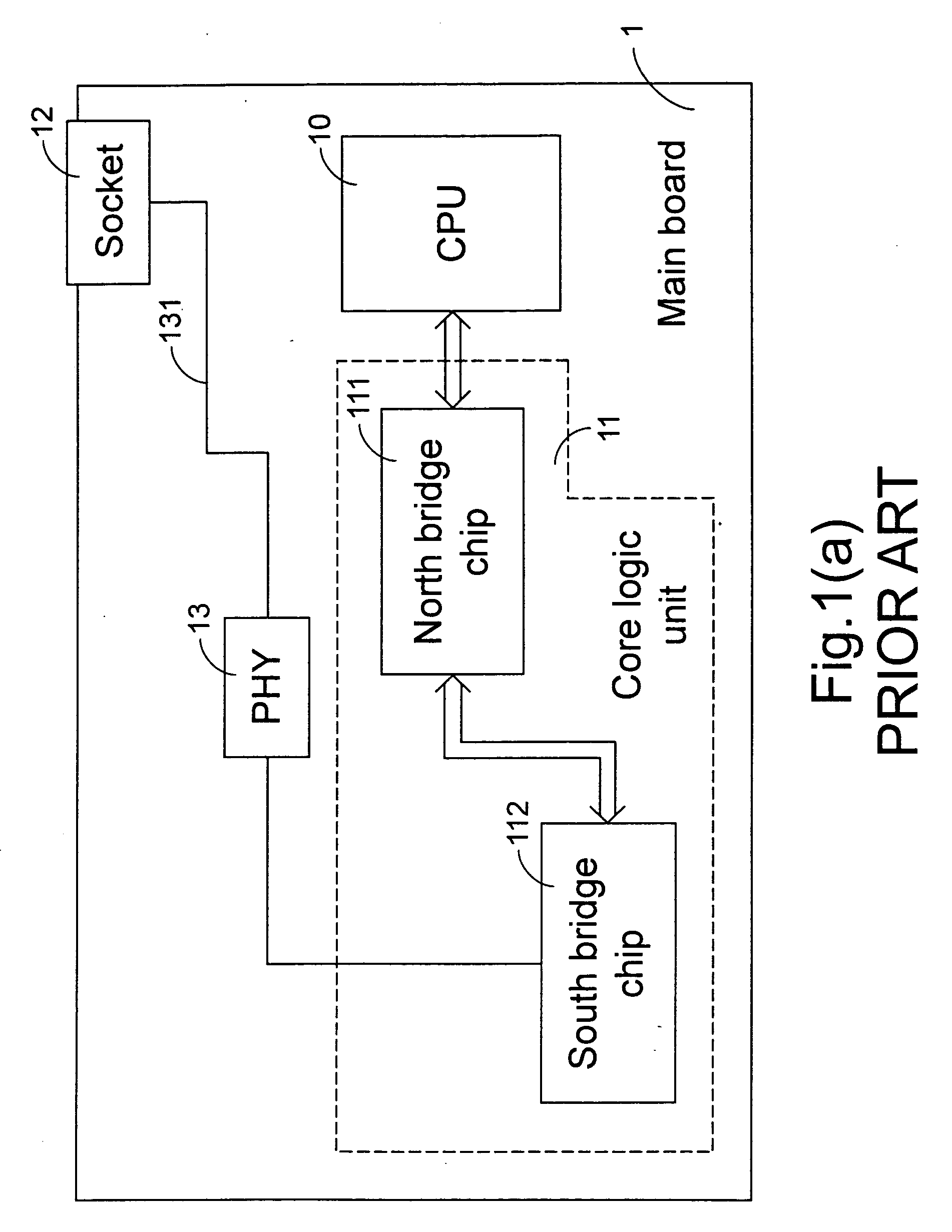
Since the trace 131 is used as a transmission line for transmitting analog signals with high frequency, the great length thereof is disadvantageous for impedance control due to possible return loss and insertion loss.
In addition, the switching power supply (not shown) disposed on the main board may interfere with the high-frequency analog signals transmitted on the main board.

Method used


Image

  • Integrated network-port socket and physical-layer device and main board incorporating the same
  • Integrated network-port socket and physical-layer device and main board incorporating the same
  • Integrated network-port socket and physical-layer device and main board incorporating the same

Examples


Embodiment Construction

[0027] Please refer to FIG. 2(a). The main board comprises a central processing unit (CPU) 20, a core logic unit 21 including a north bridge chip 211 and a south bridge chip 212, a socket 22 for receiving therefrom an external signal line and an analog circuit control chip 23 communicating with the socket 22 via an analog signal line 25 but communicating with the south bridge chip 212 via a digital signal line 24, all of which are disposed on a main body 2 of the main board.

[0028] In this embodiment, the analog circuit chip 23 is disposed in the vicinity of the socket 22 for minimizing the return loss and insertion loss while being kept at least a certain distance away from the CPU 20 to prevent from interfering with the high-frequency analog signals transmitted on the main board. For example, the distance between the analog circuit chip 23 and the CPU 20 could be greater than 100 or at least 10 times of the distance between the analog circuit chip 23 and the socket 22.

[0029] Sinc...


PUM


Abstract

A signal-line socket includes a housing, a circuit board, a socket terminal and a signal pin. The housing has a socket hole for receiving a plug of an external signal line. The circuit board is disposed in the housing and has room for mounting thereon an analog circuit chip. The socket terminal is electrically connected to the circuit board and exposed from the socket hole to be electrically connected to the plug of the external signal line for connecting the network signal line to the analog circuit chip. The signal pin is electrically connected to the circuit board and exposed from the housing to be electrically connected to a main board of a computer for connecting the analog circuit chip to the main board of the computer.

Description

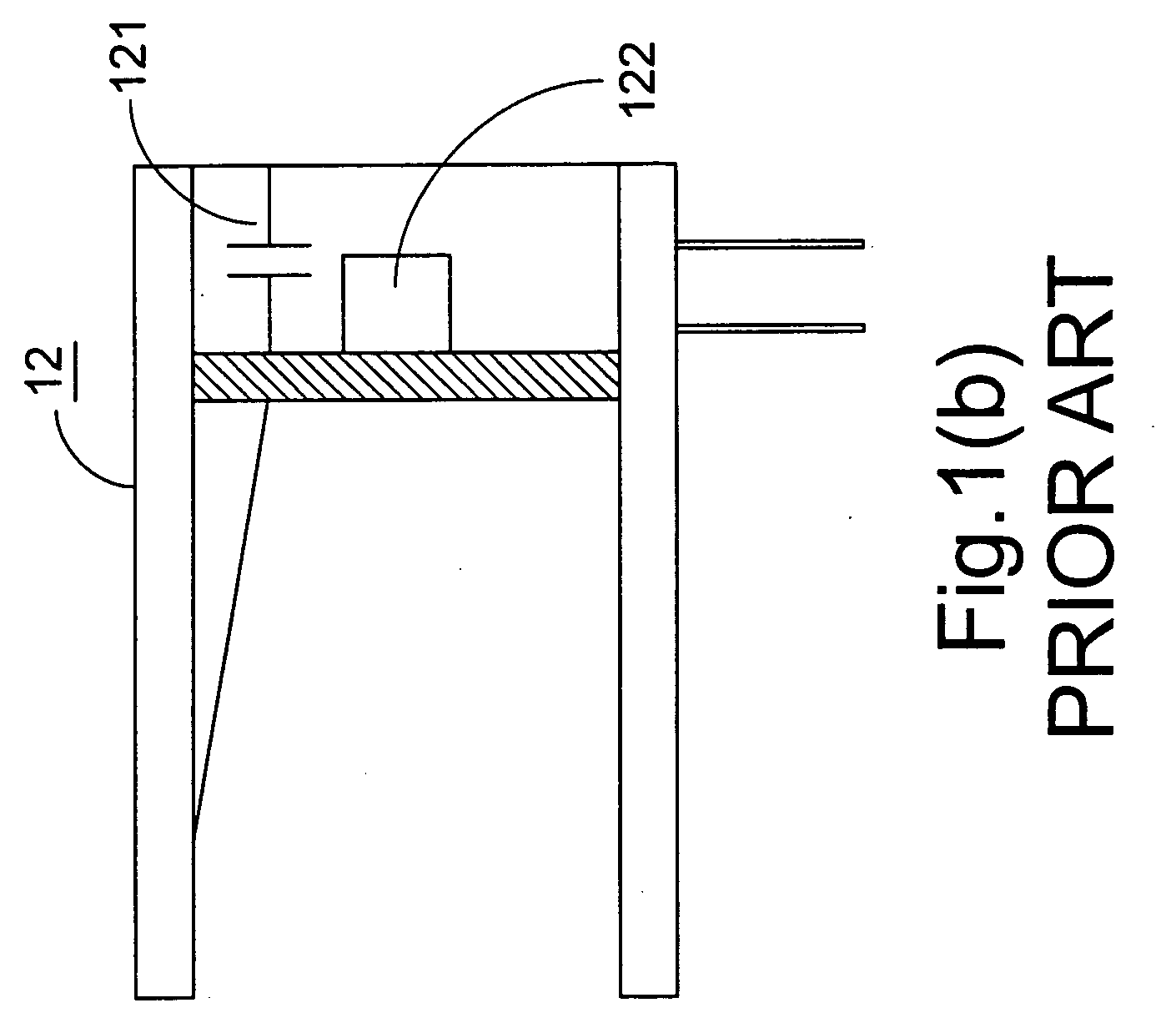
FIELD OF THE INVENTION [0001] The present invention relates to a socket structure, and particularly to a network-port socket structure for use in a computer host to communicate with the external. The present invention also relates to a main board having such socket structure. BACKGROUND OF THE INVENTION [0002]FIG. 1(a) is a schematic diagram illustrating the relative locations of a central processing unit (CPU) 10, a core logic unit 11 including a north bridge chip 111 and a south bridge chip 112, a high-speed Ethernet socket 12 and a physical layer (PHY) chip 13, all of which are mounted on a main board 1. The high-speed Ethernet socket 12 is also usually referred to as an RJ-45 socket. A conventional high-speed Ethernet socket 12 shown in FIG. 1(b) comprises a high-voltage resistant capacitor 121 and a transformer 122. The PHY chip 13 is conventionally designed to be distant from the CPU 10 as far as possible for avoiding interference of heat and noise generated during the operati...

Claims


Application Information

Patent Timeline
IPC IPC(8): G01R31/02H01R13/66H01R24/06
CPCH01R13/6658
Inventor PENG, HSI-CHIHLEE, CAMILLE
Owner VIA TECH INC
Learn More