
Optical processing

a technology of optical devices and optical processing, applied in multiplex communication, manufacturing tools, instruments, etc., can solve the problems of providing different alignment errors, critical source of system failure or insertion loss, and affecting the performance of optical systems, so as to achieve the optimal performance of the system and reduce the error

Inactive Publication Date: 2005-01-27
THOMAS SWAN & CO LTD
View PDF11 Cites 35 Cited by
  • Summary
  • Abstract
  • Description
  • Claims
  • Application Information

AI Technical Summary

Benefits of technology

An advantage of the method of this aspect of the invention is that stable operation can be achieved in the presence of effects such as ageing, temperature, component, change of path through the system and assembly tolerances.
In another class of embodiments, a non-linear phase modulation profile is selected to provide beam shaping, for example so as to reduce cross-talk effects due to width clipping. This may use a pseudo amplitude modulation technique.

Problems solved by technology

Optical systems are subject to performance impairments resulting from aberrations, phase distortions and component misalignment.
An example is a multiway fibre connector, which although conceptually simple can often be a critical source of system failure or insertion loss due to the very tight alignment tolerances for optical fibres, especially for single-mode optical fibres.
Every time a fibre connector is connected, it may provide a different alignment error.
Another example is an optical switch in which aberrations, phase distortions and component misalignments result in poor optical coupling efficiency into the intended output optical fibres.
This in turn may lead to high insertion loss.
The aberrated propagating waves may diffract into intensity fluctuations creating significant unwanted coupling of light into other output optical fibres, leading to levels of crosstalk that impede operation.
In some cases, particularly where long path lengths are involved, the component misalignment may occur due to ageing or temperature effects.
For example in a communications context, known free-space wavelength multiplexers and demultiplexers use expensive thermally stable opto-mechanics to cope with the problems associated with long path lengths.
The prior art does not adequately address this situation.
In such systems, effects such as assembly errors, manufacturing tolerances in the optics and also changes in the system behaviour due to temperature and ageing, create the desirability for dynamic direction control, aberration correction, phase distortion compensation or misalignment compensation.

Method used


Image

  • Optical processing
  • Optical processing
  • Optical processing

Examples


second embodiment

In a second embodiment a further linear phase modulation is applied to the hologram during each stage so as to deflect the beam to be measured while taking the moments towards a particular photodiode.

Consider a Gaussian type beam b(u,v) centred at position co-ordinates (u0,v0). The even symmetry of the beam about axes parallel to the u and v directions and through the centre lead to the identities given by equations (36) and (37).

∫∫(u−u0)b(u,v)du dv=0  (36)

∫∫(v−v0)b(u,v)du dv=0  (37)

Hence approximate values of the first order moments measured as described previously, or by some other method, may be used to deduce approximate positions for the beam centres, as shown by equations (38) and (39). u0≈a1⁢Ua0(38)v0≈a1⁢Va0(39)

In the next stage of the measurement the pixel block initially assigned to the beam is re-assigned such that it is centred within half a pixel in each of the u and v directions from the approximate centre of the beam, as just calculated.

Let the new centre of the ...

third embodiment

In a third embodiment the input beam could contain one or more signals spread almost continuously across the wavelength range. The light at a particular wavelength will be incident over a small transverse region of the SLM, with, typically a Gaussian type spatial distribution of energy against position. The position of the peak in the spatial distribution is wavelength dependent and may be calculated from the grating and lens properties. For such a system the beam deflection or channel equalisation varies continuously with wavelength. The pixellated SLM is divided into blocks, each characterised by a ‘central wavelength’, defined by the wavelength whose spatial peak lands in the middle of the block. A particular channel equalisation or beam deflection is applied uniformly across this block. Light of a wavelength with a spatial peak landing in between the centres of two blocks will see a system response averaged across the two blocks. As the spatial peak moves towards the centre of o...


PUM

PropertyMeasurementUnit
Temperatureaaaaaaaaaa
Poweraaaaaaaaaa
Electric potential / voltageaaaaaaaaaa

Abstract

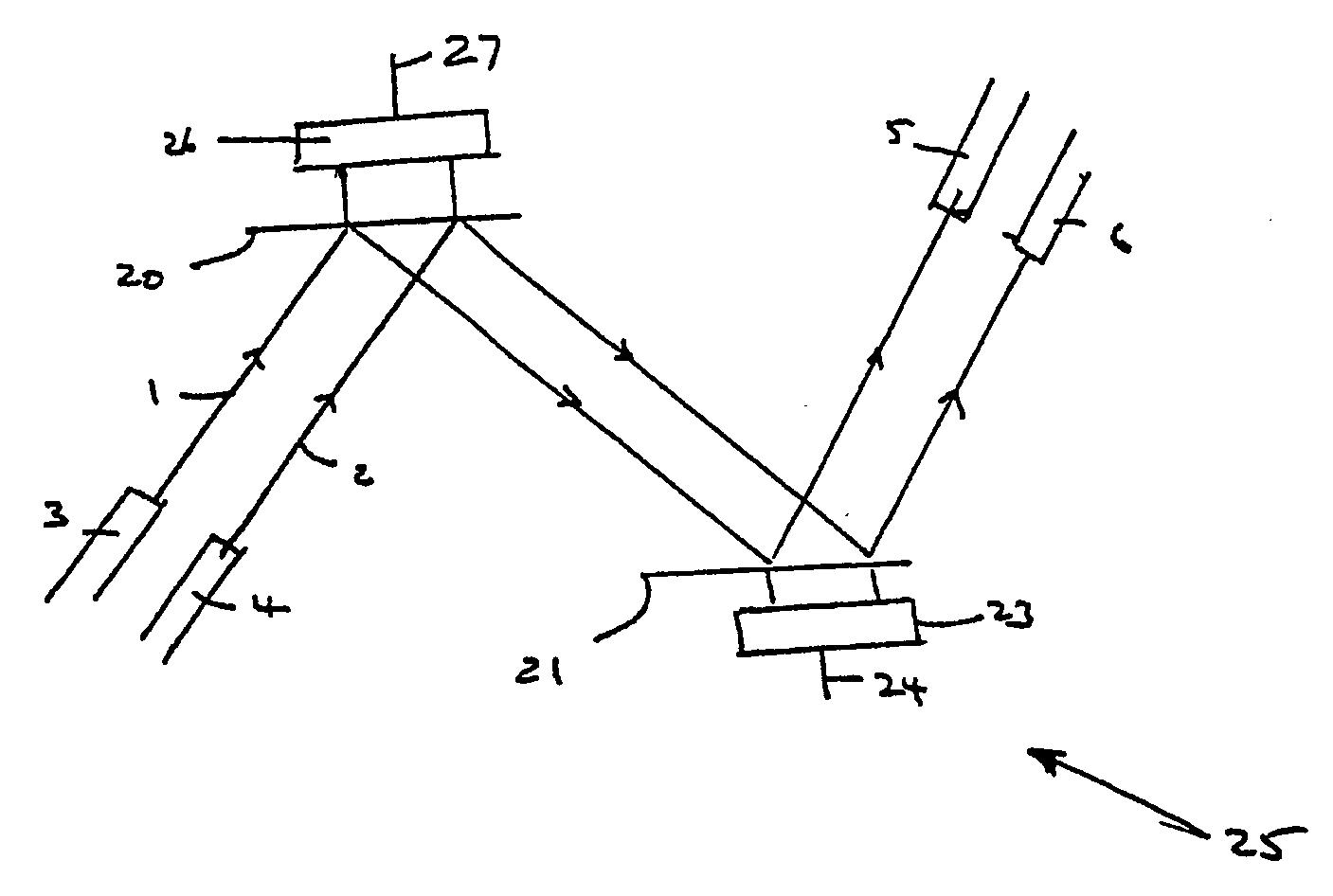
To operate an optical device comprising an SLM with a two-dimensional array of controllable phase-modulating elements groups of individual phase-modulating elements are delineated, and control data selected from a store for each delineated group of phase-modulating elements. The selected control data are used to generate holograms at each group and one or both of the delineation of the groups and the selection of control data is / are varied. In this way upon illumination of the groups by light beams, light beams emergent from the groups are controllable independently of each other.

Description

FIELD OF THE INVENTION The present invention relates to an optical device and to a method of controlling an optical device. More particularly but not exclusively the invention relates to the general field of controlling one or more light beams by the use of electronically controlled devices. The field of application is mainly envisaged as being to fields in which reconfiguration between inputs and outputs is likely, and stability of performance is a significant requirement. BACKGROUND OF THE INVENTION It has previously been proposed to use so-called spatial light modulators to control the routing of light beams within an optical system, for instance from selected ones of a number of input optical fibres to selected ones of output fibres. Optical systems are subject to performance impairments resulting from aberrations, phase distortions and component misalignment. An example is a multiway fibre connector, which although conceptually simple can often be a critical source of syste...

Claims


Application Information

Patent Timeline
IPC IPC(8): G02B5/32G02B6/26G02B6/34G02B6/35G02F1/31G03H1/08H04J14/08H04Q11/00
CPCG02B5/32G02F2203/12G02B6/29311G02B6/29314G02B6/29391G02B6/3512G02B6/3534G02B6/3548G02B6/3556G02F1/31G03H1/0005G03H1/02G03H1/08G03H1/2294G03H2001/0224G03H2001/0491G03H2001/261G03H2222/32G03H2225/32G03H2225/52G03H2226/02H04J14/021H04J14/0212H04J14/0213H04J14/0217H04J14/0219H04J14/022H04J14/08H04Q11/0005H04Q2011/0028H04Q2011/0039G03H1/2286G03H2222/13G03H2223/23G03H1/04G03H1/0891G02F1/13342G02F2203/50G02F2203/28G02F1/01G03H1/0866G02F1/1335G02F1/29G02F2001/291G02F2201/30G02F2201/34G02B6/266G02F1/3132G03H2225/60G02F1/291G02B6/2938G02B26/06G02B26/0808G02B26/0833G02F1/1326G03H1/26G03H2001/264H04Q2011/0016
Inventor HOLMES, MELANIE
Owner THOMAS SWAN & CO LTD
Learn More