
Portable device and semiconductor device

a technology of semiconductor devices and portable devices, applied in transportation and packaging, secondary cell servicing/maintenance, safety/protection circuits, etc., can solve the problems of battery deterioration, battery charging capacity greatly affected by charging voltage, and portable devices with more functions and compactness

Active Publication Date: 2005-01-27
MONTEREY RES LLC
View PDF3 Cites 69 Cited by
  • Summary
  • Abstract
  • Description
  • Claims
  • Application Information

AI Technical Summary

Benefits of technology

"The present invention relates to a portable device that can be connected to a battery pack including a secondary battery. The device has a charging circuit that includes a charging terminal and a voltage detection terminal to charge the battery. The charging circuit stops charging if there is a voltage abnormality detected at the voltage detection terminal. The invention also includes a semiconductor device that generates a current detection signal and a charge control signal to control the charging process. The charge control signal stops charging if there is an abnormal voltage at the voltage detection terminal. The method also involves connecting the battery pack to the portable device and stopping the supply of charging current if there is an abnormal voltage at the second voltage detection terminal. The technical effects of the invention include improving the safety and reliability of charging portable devices with battery packs."

Problems solved by technology

However, recent portable devices have more functions and are becoming more compact.
When using a lithium ion battery in a portable device, the charging capacity of the battery is greatly affected by the charging voltage.
The battery deteriorates when the charging voltage is too high, and overdischarging makes it difficult for the battery to function properly.
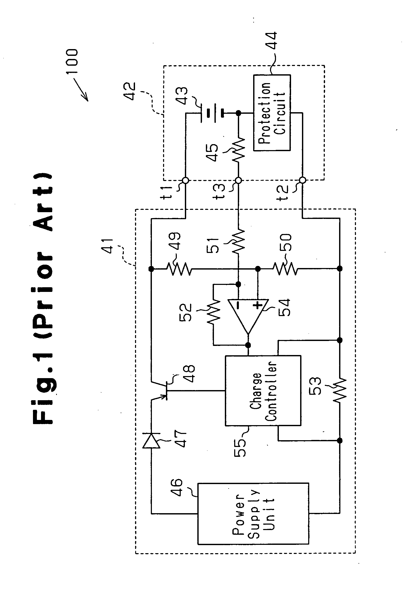
Thus, there is always the possibility of contact failure with the charging circuit 41.
This hinders charging with the constant voltage.

Method used


Image

  • Portable device and semiconductor device
  • Portable device and semiconductor device
  • Portable device and semiconductor device

Examples


Embodiment Construction

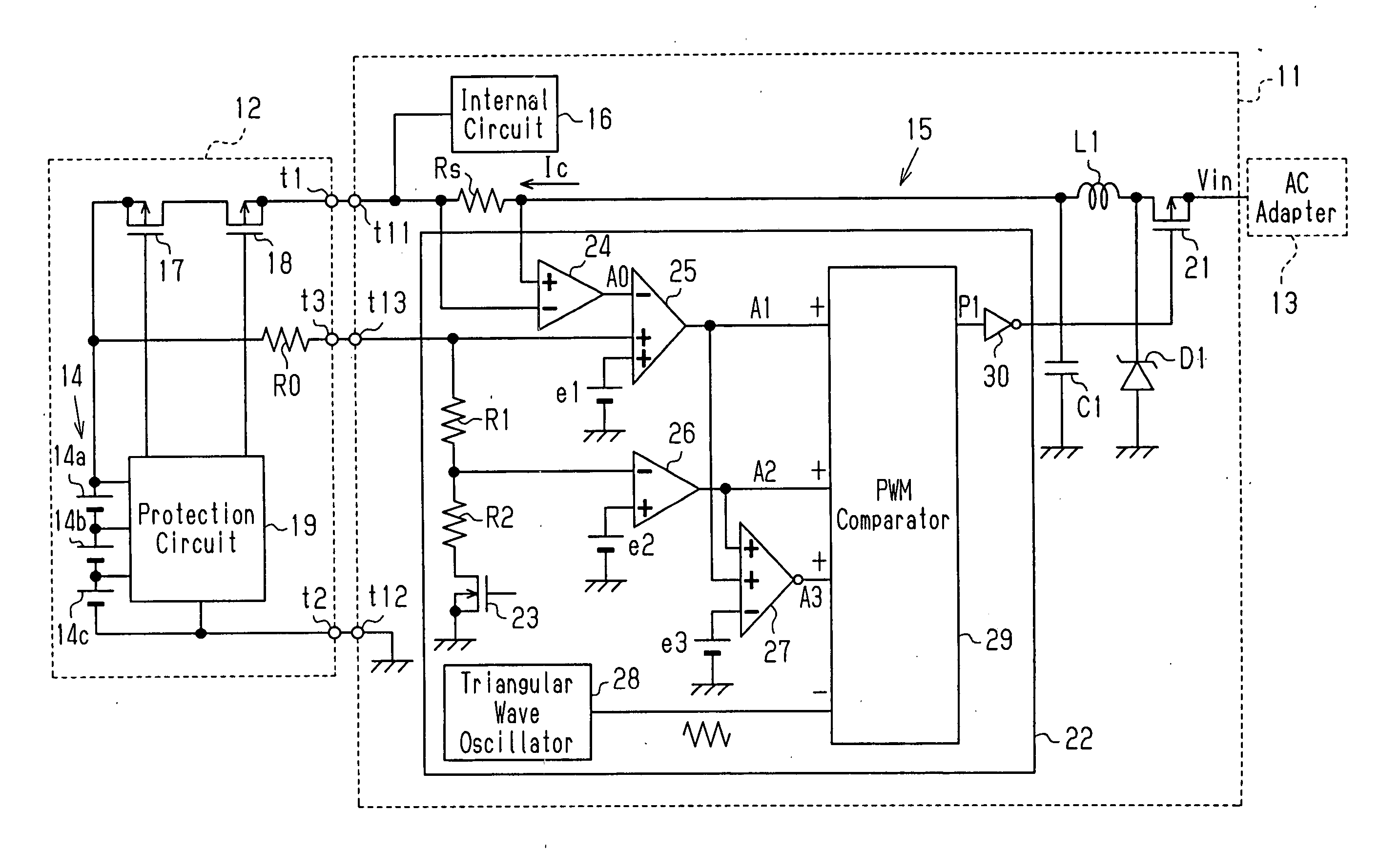
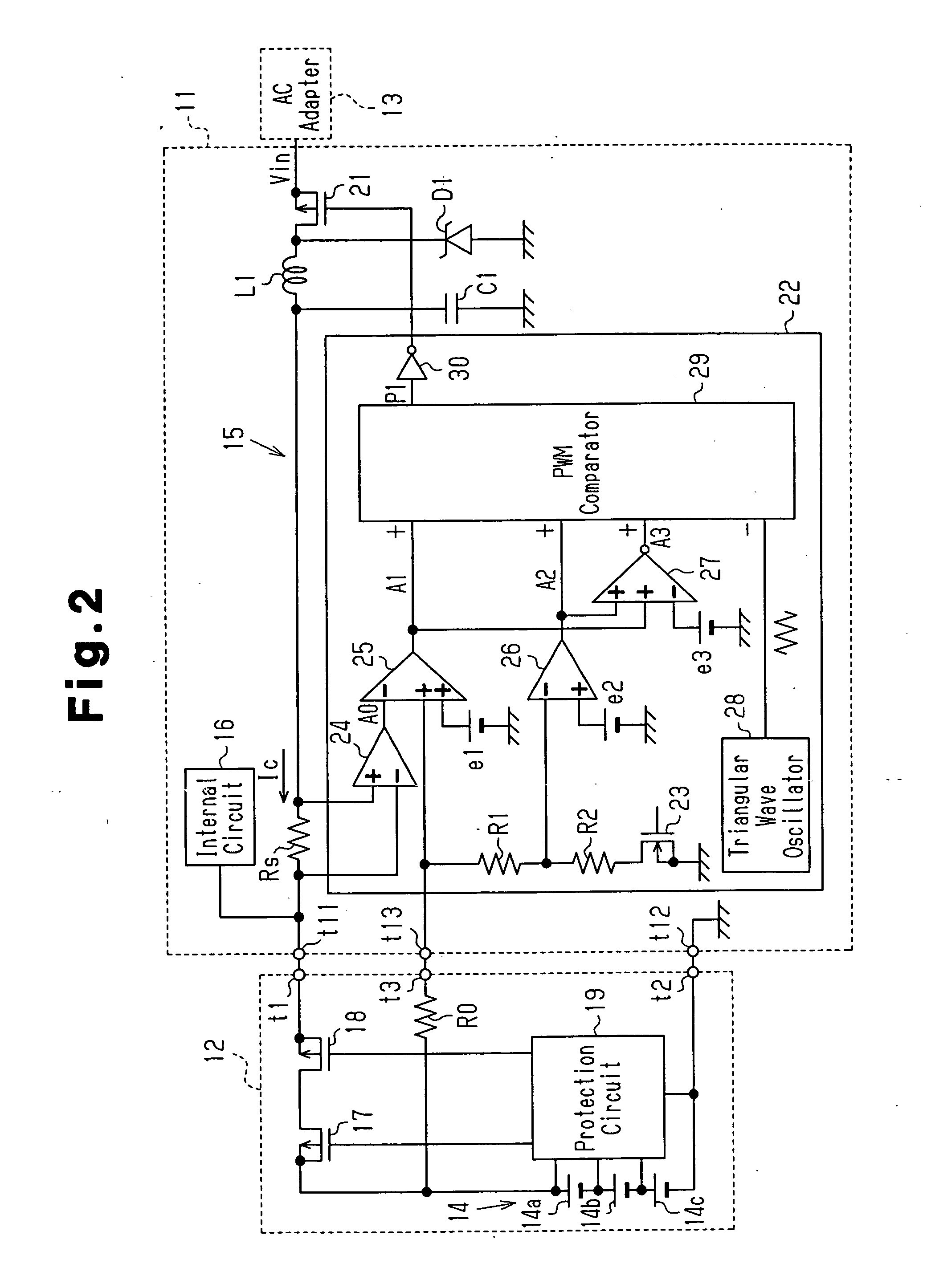
[0020] In the drawings, like numerals are used for like elements throughout. FIG. 2 is a schematic circuit diagram of a portable device (notebook computer) 11 according to a preferred embodiment of the present invention.

[0021] A battery pack 12 is connected to the portable device 11. The portable device 11 is connected to an AC adapter 13, which serves as an external power supply. The portable device 11 includes a charging circuit 15 for charging a secondary battery 14, which is incorporated in the battery pack 12, and an internal circuit 16, which is operated by the battery voltage of the secondary battery 14. The internal circuit 16 includes a microcomputer, which centrally controls the portable device 11, and its peripheral circuits.

[0022] The battery pack 12 is detachably connected to the portable device 11. When the battery pack 12 is connected to the portable device 11, the charging circuit 15 charges the secondary battery 14. The secondary battery 14 of the battery pack 12 ...


PUM

PropertyMeasurementUnit
voltageaaaaaaaaaa
battery voltageaaaaaaaaaa
voltageaaaaaaaaaa

Abstract

A portable device for preventing overcharging of a secondary battery resulting from contact failure of a voltage detection terminal. The portable device includes a charging circuit for charging the secondary battery when a battery pack, which includes the secondary battery, is connected to the portable device. The charging circuit includes a charging terminal, which is used to supply the secondary battery with charging current, and a voltage detection terminal, which is used to detect voltage of the secondary battery. The charging circuit stops charging the secondary battery when voltage abnormality is detected at the voltage detection terminal.

Description

CROSS-REFERENCE TO RELATED APPLICATIONS [0001] This application is based upon and claims the benefit of priority from the prior Japanese Patent Application No. 2002-270952, filed on Sep. 18, 2002, the entire contents of which are incorporated herein by reference. BACKGROUND OF THE INVENTION [0002] The present invention relates to a portable device having a charging circuit for charging a secondary rechargeable battery incorporated in a detachable battery pack and to a semiconductor device configuring the charging circuit. [0003] Portable devices, such as a notebook computer, a personal digital assistant (PDA), and a cellular phone, use battery packs. A battery pack includes a secondary battery. A lithium ion battery is often employed as the secondary battery. The lithium ion battery is advantageous in that it decreases the operation cost of devices using the battery and in that it enables a large amount of current to be instantaneously discharged. A device employing a secondary batt...

Claims


Application Information

Patent Timeline
Patent Type & Authority Applications(United States)
IPC IPC(8): G06F1/28H01M10/44H02H7/18H02J7/00H04M1/02
CPCH02J7/0031H02J7/02H02J2207/20
Inventor TAKIMOTO, KYUICHIOZAWA, HIDEKIYO
Owner MONTEREY RES LLC
Learn More