
Solid-state imaging device and method for driving the same

a solid-state imaging and imaging device technology, applied in the direction of instrumentation, color signal processing circuit, radioation controlled devices, etc., can solve the problems of low power consumption, difficult to raise the driving frequency, and limit the driving frequency characteristics of a ccd image sensor, so as to improve the frame rate, reduce the need for unnecessary data, and simplify the structure

Inactive Publication Date: 2005-01-27
SHARP KK
View PDF3 Cites 11 Cited by
  • Summary
  • Abstract
  • Description
  • Claims
  • Application Information

AI Technical Summary

Benefits of technology

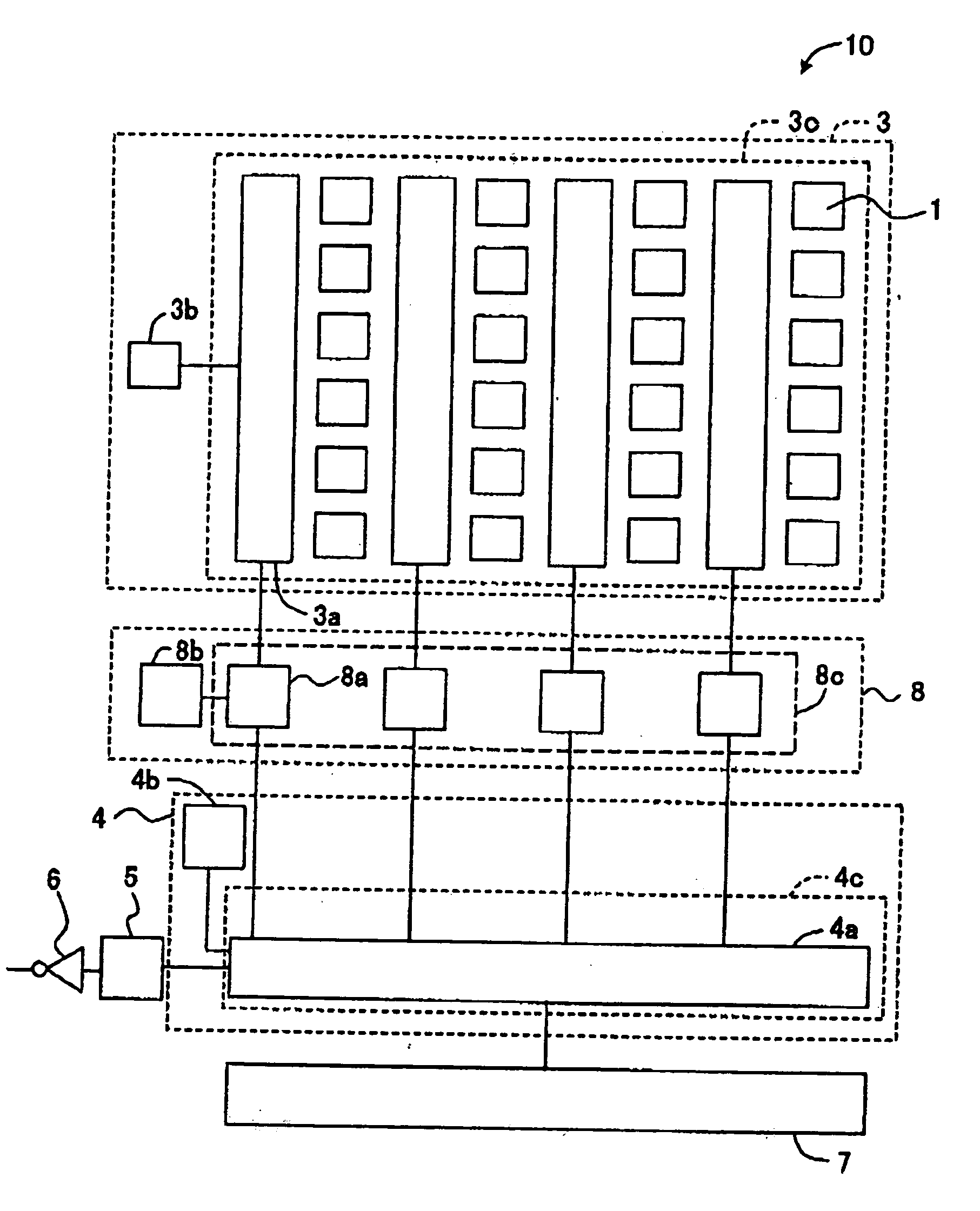
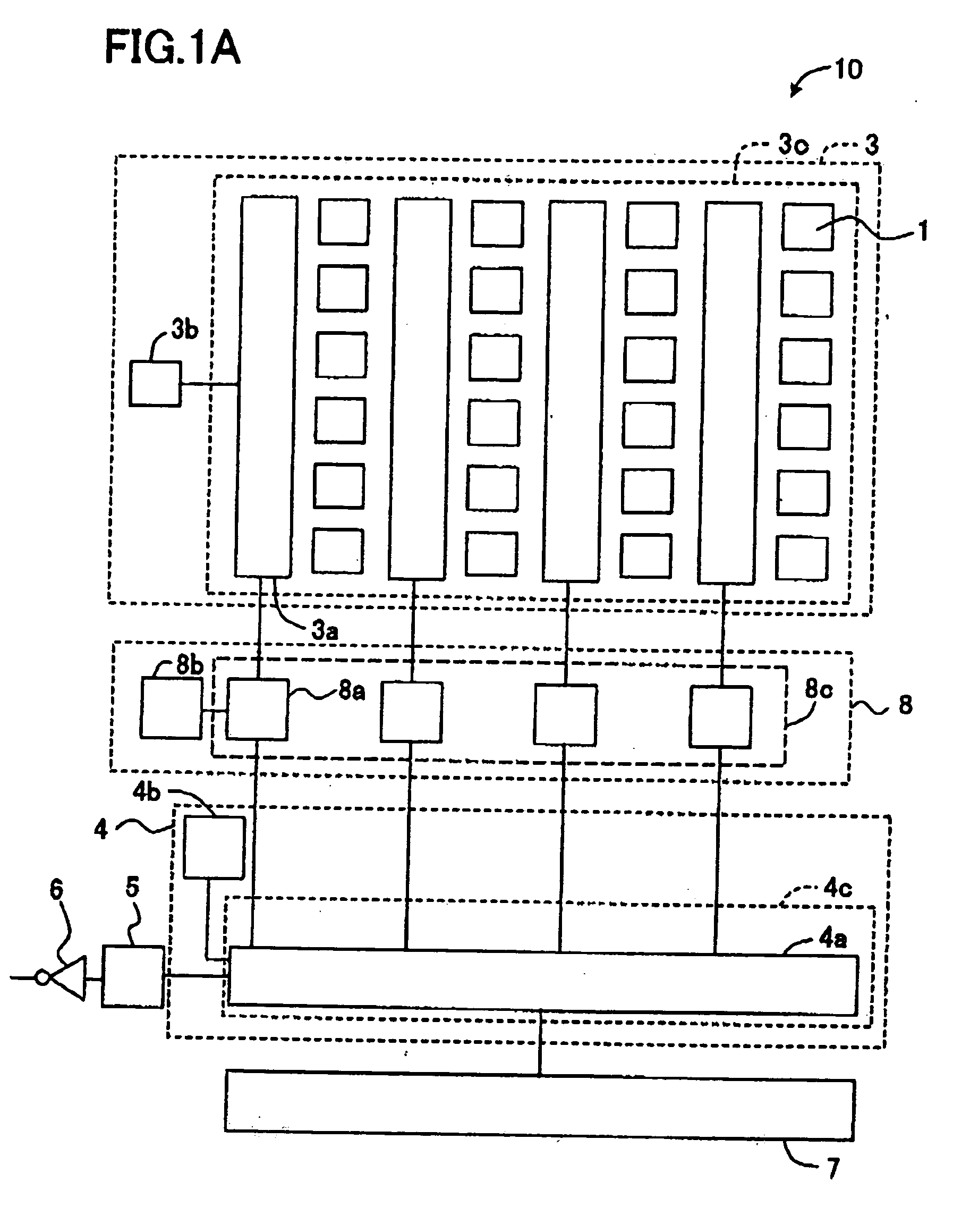
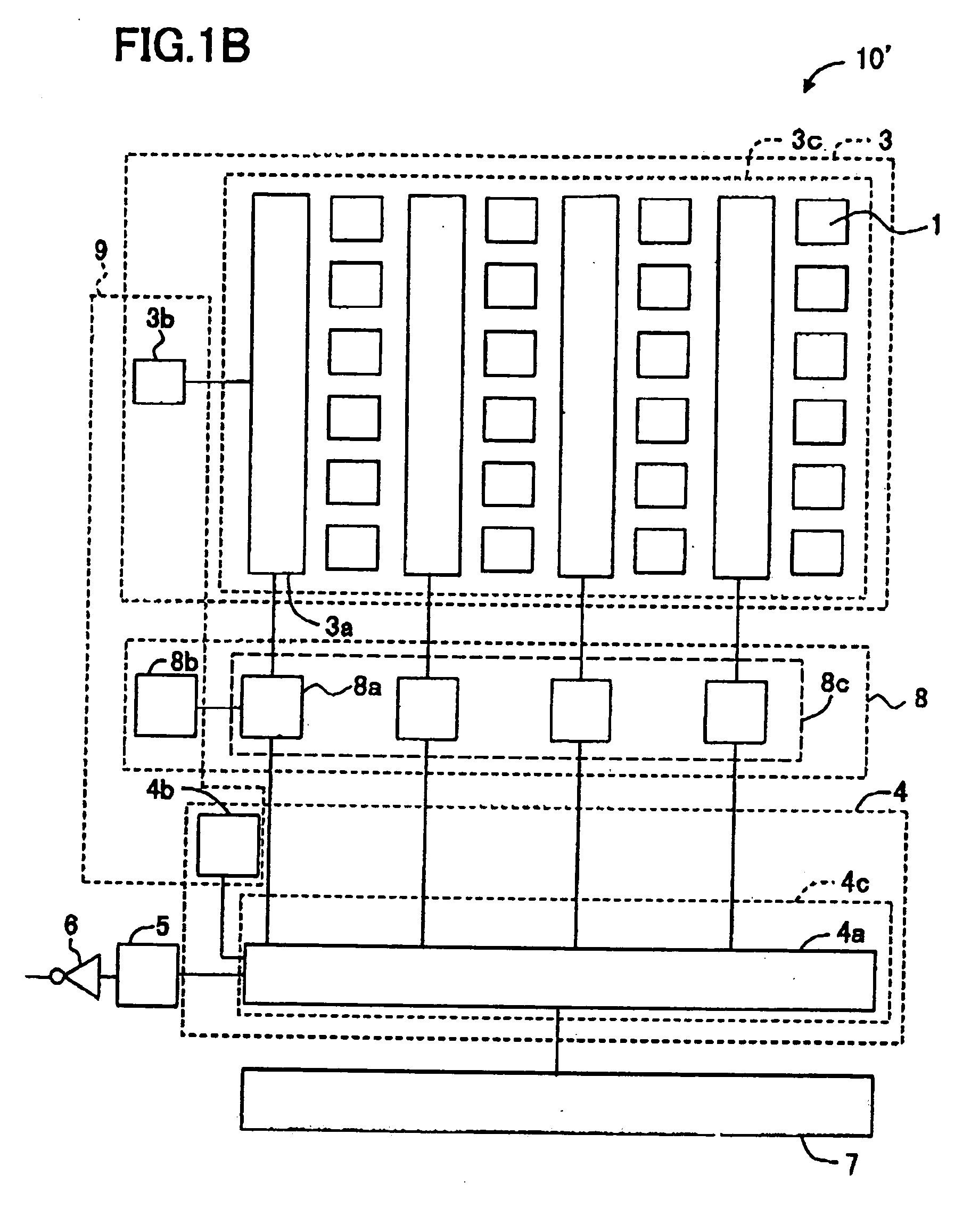
The invention is a solid-state imaging device with a matrix of light receiving sections and a vertical transfer register section for transferring charges from the light receiving sections to a horizontal transfer register section. A dummy area transfer register section is included for transferring charges in a vertical direction and a horizontal direction. The device also includes a control section for controlling the transfer of charges in both the vertical and horizontal directions. The technical effect of the invention is to provide a more efficient and flexible solid-state imaging device with improved transfer of charges and control over the transfer of charges in both directions.

Problems solved by technology

However, there is a limit in the driving frequency characteristics of a CCD image sensor, and a low power consumption is demanded.
Therefore, it in not easy to raise the driving frequency.
This makes it difficult to obtain the necessary frame rate in the monitoring mode as the number of pixels of a CCD image sensor increases.
For data removal in the horizontal direction, the methods have the following problems.
This is very difficult.
However, in this case, the discharge operation of the charges is performed at a time, unnecessary data in the horizontal direction cannot be selectively removed.
In order to perform the method of adding the signals of the some color which are adjacent in the horizontal direction with the conventional data removal methods, it is necessary to control the signal read from the vertical transfer registers to the horizontal transfer register column by column, such that there in a delay in the time to read the signals.
In addition, the solid-state imaging device disclosed in this publication requires a three-layer electrode, which complicates the production process.
Therefore, the structure of the solid-state imaging device is complicated.

Method used


Image

  • Solid-state imaging device and method for driving the same
  • Solid-state imaging device and method for driving the same
  • Solid-state imaging device and method for driving the same

Examples


example 1

[0122]FIG. 1C is a schematic plan view illustrating a structure of a CCD image sensor 10A according to a first example of the present invention. For the sake of simplicity, FIG. 1C omits the pixel area transfer control section 3b, the dummy area transfer control section 8b, and the horizontal transfer control section 4b (FIG. 1A). FIG. 1C also omits the control section 9 (FIG. 1B).

[0123] As Shown in FIG. 1C, the CCD image sensor 10A includes a plurality of photodiodes 1 (pixels) arranged in six rows and four columns.

[0124] As shown in FIG. 1C, the CCD image sensor 10A is an interline transfer type CCD image sensor having six-phase driving vertical transfer registers which are produced by a simple two-layer gate process.

[0125] The plurality of photodiodes 1 are arranged in a matrix (i.e., a plurality of rows and a plurality of columns, as described above), in the pixel area on a semiconductor substrate. A top view of each photodiode 1 is covered with a color filter of R, G or B. T...

example 2

[0171]FIG. 6 in a schematic plan view illustrating a structure of a CCD image sensor 10B according to a second example of the present invention. The CCD image sensor 10B includes a plurality of photodiodes 1 each acting as a light receiving section, transfer gates 2, pixel area vertical transfer registers 3a, a horizontal transfer register 4a, dummy area vertical transfer registers 8a, a charge detection section 5, an output amplifier 6, and a sweep-out drain 7. These elements have the same structure and function in the same manner as those described in the first example, and will not be described in detail here.

[0172] For the sake of simplicity, FIG. 6 omits the pixel area transfer control section 3b, the dummy area transfer control section 8b, and the horizontal transfer control section 4b (FIG. 1A). FIG. 6 also omits the control section 9 (FIG. 1B).

[0173] As shown in FIG. 6, the CCD image sensor 10B includes a plurality of photodiodes 1 (pixels) arranged in four rows and six co...

example 3

[0228]FIG. 11 is a schematic plan view illustrating a structure of a CCD image sensor 10C according to a third example of the present invention. The CCD image sensor 10C includes a plurality of photodiodes 1 each acting as a light receiving section, transfer gates 2, pixel area vertical transfer registers 3a, a horizontal transfer register 4a, dummy area vertical transfer registers 8a, a charge detection section 5, an output amplifier 6, and a sweep-out drain 7. These elements have the same structure and function in the same manner as those described in the first example, and will not be described in detail here.

[0229] For the sake of simplicity, FIG. 11 omits the pixel area transfer control section 3b, the dummy area transfer control section 8b, and the horizontal transfer control section 4b (FIG. 1A). FIG. 11 also omits the control section 9 (FIG. 1B).

[0230] As shown in FIG. 11, the CCD image sensor 10C includes a plurality of photodiodes 1 (pixels) arranged in five rows and fou...


PUM


Abstract

A solid-state imaging device including a plurality of light receiving sections; a pixel area vertical transfer register section for transferring, column by column, charges generated by the plurality of light receiving sections; a dummy area vertical transfer register section for transferring, column by column in the vertical direction, the charges which have been transferred by the pixel area vertical transfer register section, the dummy area vertical transfer register section providing a control such that the transfer of the charges of at least one of the plurality of columns is performed in the same manner as the charges in the other columns in one case, and in a different manner from the transfer of the charges in the other columns in another case; and a horizontal transfer register section for transferring, in a horizontal direction, the charges which have been transferred from the dummy area vertical transfer register section.

Description

[0001] This non-provisional application claims priority under 35 U.S.C., §119(a), on Patent Application No. 2003-275021 filed in Japan on Jul. 15, 2003, the entire contents of which are hereby incorporated by reference.BACKGROUND OF THE INVENTION [0002] 1. Field of the Invention [0003] The present invention relates to a solid-state imaging device and a method for driving the same, and in particular to a solid-state imaging device usable as an imaging device for a digital still camera, a video camera or the like, and a method for driving the same. [0004] 2. Description of the Related Art [0005] Recently, the image quality of digital still cameras has been rapidly enhanced. As an imaging device therefor, solid-state imaging devices, especially CCD image sensors having a pixel number of one million or greater have been widely used. These CCD image sensors are generally switchable between two driving modes, i.e., a still mode in which a signal charge is independently read from all the p...

Claims


Application Information

Patent Timeline
Patent Type & Authority Applications(United States)
IPC IPC(8): H01L21/339H01L27/00H01L27/148H01L29/762H04N25/00
CPCH01L27/14812H01L27/14621H01L27/146H04N25/73
Inventor OZUMI, TAKEHIKO
Owner SHARP KK
Learn More