Semiconductor memory device and electronic device
a memory device and semiconductor technology, applied in the field of word line activation control, can solve the problems of increasing the possibility of data loss, requiring a long time to refresh, and being more expensive and small in capacity, so as to eliminate the long time restriction of a semiconductor memory devi
- Summary
- Abstract
- Description
- Claims
- Application Information
AI Technical Summary
Benefits of technology
Problems solved by technology
Method used
Image

Examples
Embodiment Construction
One mode of carrying out the invention is discussed below as a preferred embodiment in the following sequence:
A. Terminal Structure of Semiconductor Memory Device and Outline of Working State
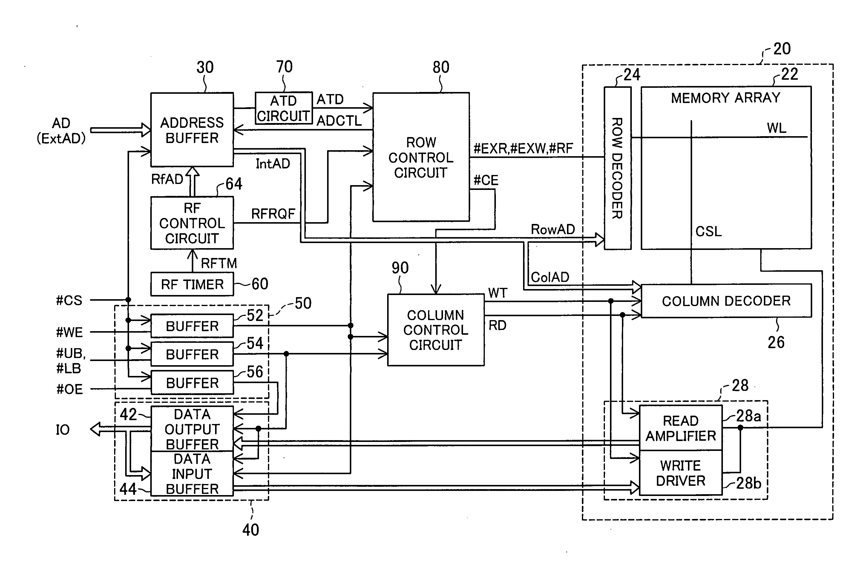
B. Internal Structure of Semiconductor Memory Device
B1. General Structure
B2. Row Control Circuit B.2.1 Read Execution Signal Generator B.2.2 Write Execution Signal Generator B.2.3 Refresh Execution Signal Generator B.2.4 Operations of Respective Generators
B3. Address Buffer and Data Input Buffer B.3.1 Address Buffer B.3.2 Data Input Buffer
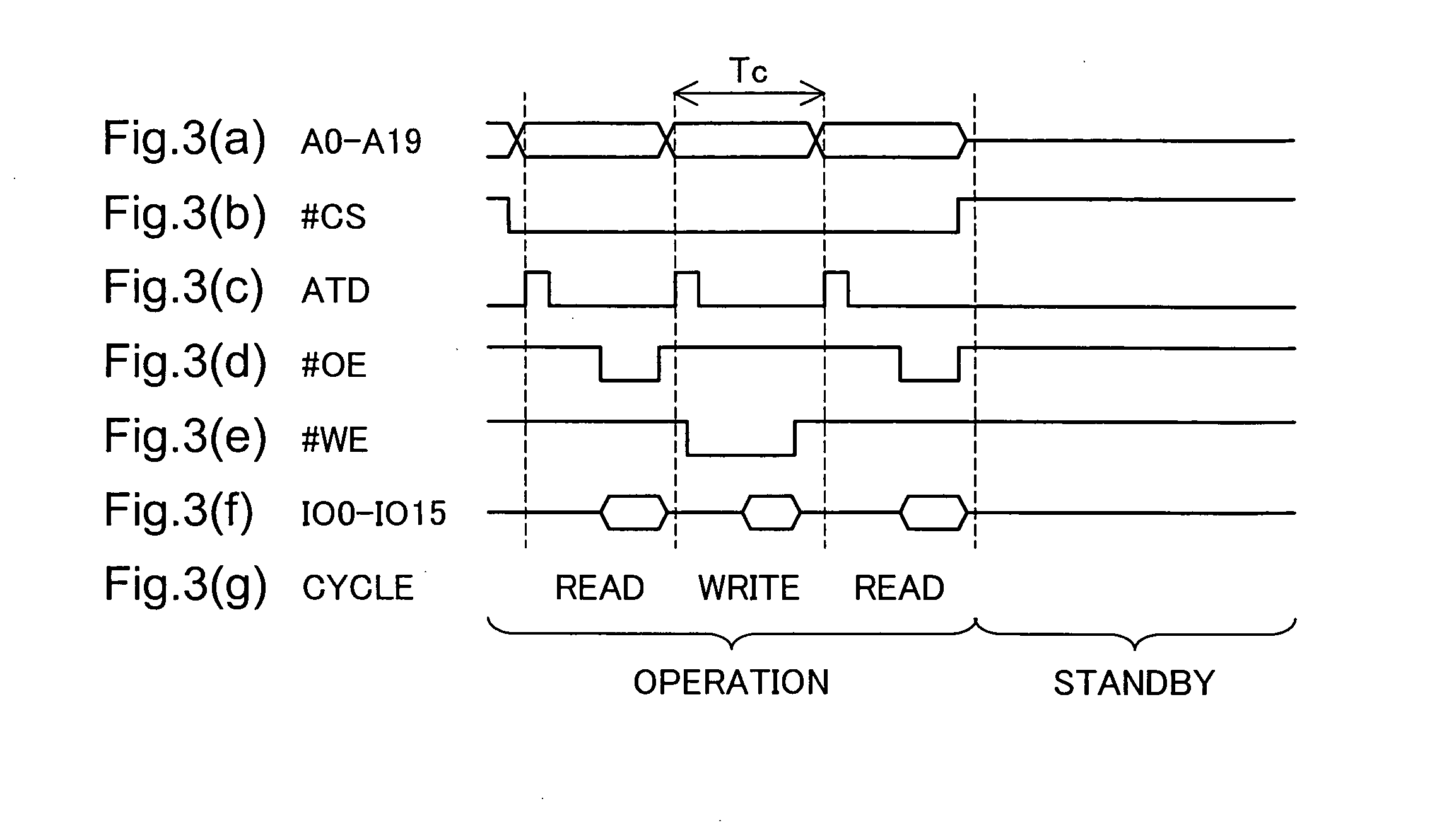
C. Operations in Operation Mode
C1. Read Access
C2. Early Write Access
C3. Delay Write Access
D. Application to Electronic Device
E. Modification
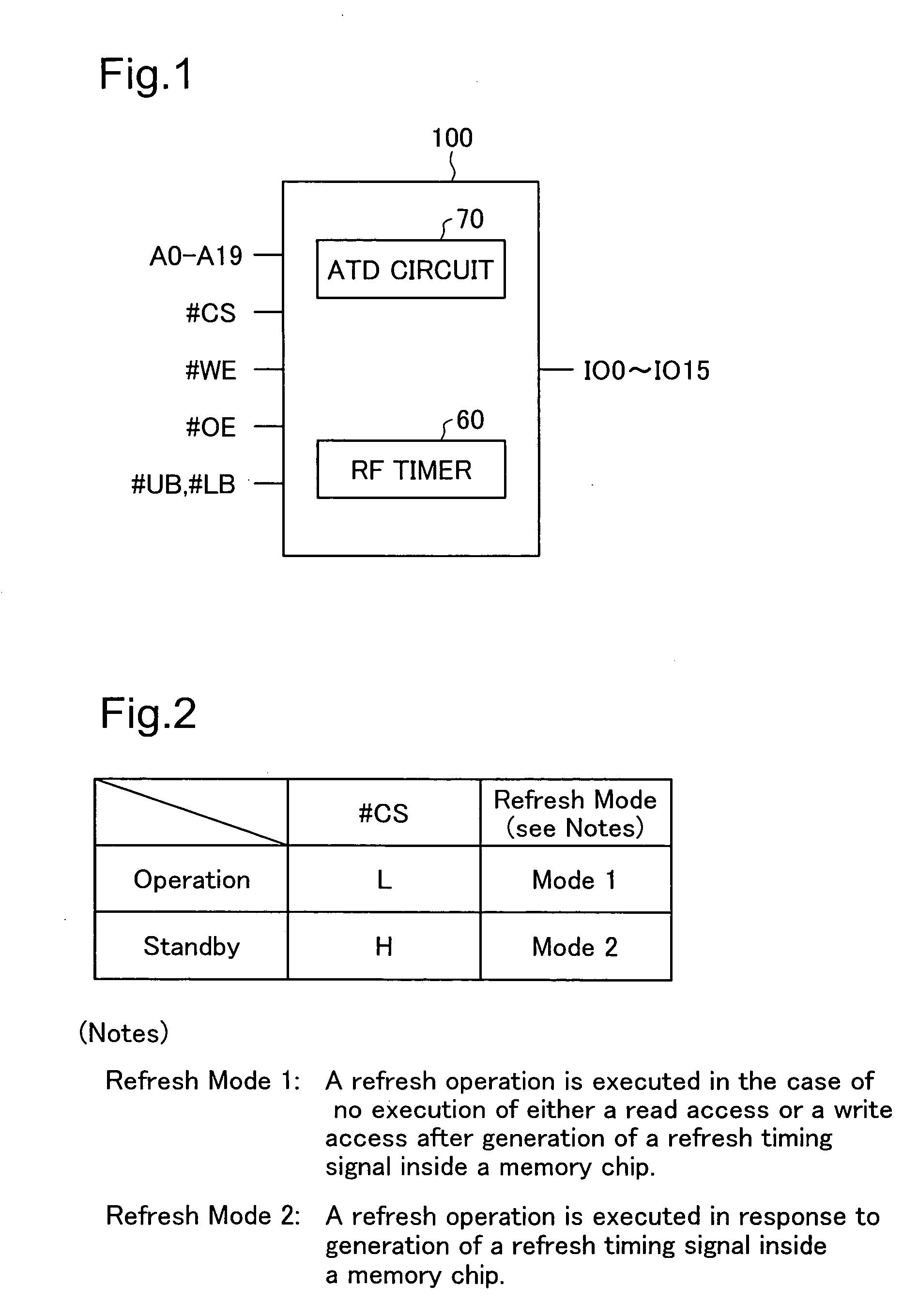
A. Terminal Structure of Semiconductor Memory Device and Outline of Working State
FIG. 1 shows the terminal structure of a memory chip 100 in one embodiment of the semiconductor memory device of the invention. The memory chip 100 has terminals given below:
A0 to A19: 20 Address Input Terminal...
PUM
 Abstract
Description
Claims
Application Information
 - R&D
- Intellectual Property
- Life Sciences
- Materials
- Tech Scout
- Unparalleled Data Quality
- Higher Quality Content
- 60% Fewer Hallucinations
Browse by: Latest US Patents, China's latest patents, Technical Efficacy Thesaurus, Application Domain, Technology Topic, Popular Technical Reports.
© 2025 PatSnap. All rights reserved.Legal|Privacy policy|Modern Slavery Act Transparency Statement|Sitemap|About US| Contact US: help@patsnap.com