Eureka AIR delivers breakthrough ideas for toughest innovation challenges, trusted by R&D personnel around the world.

Semiconductor apparatus with multiple delivery devices for components

a technology of semiconductor devices and components, applied in computer control, special data processing applications, program control, etc., can solve the problems of insufficient system flexibility, limited throughput (normally quantified in units per hour or "uph"), and inability to meet the needs of multiple bond heads and conveyor systems

Inactive Publication Date: 2004-12-09
ASM ASSEMBLY AUTOMATION LTD
View PDF7 Cites 37 Cited by
  • Summary
  • Abstract
  • Description
  • Claims
  • Application Information

AI Technical Summary

Benefits of technology

[0010] The invention thus seeks to provide an improved apparatus with increased throughput by utilizing multiple delivery devices to delivery materials onto a substrate without some of the aforesaid disadvantages.

Problems solved by technology

However, there is a limitation in the throughput (normally quantified in Units Per Hour or "UPH") attainable for single-head systems.
This system is not sufficiently flexible.
The space available to accommodate the multiple bond heads and conveyor system is another problem.
Moreover, since the machine is more complex with a higher number of devices, there is a higher possibility of failure.
If there is an error in aligning the positions as well as the level adjustments for each individual bond head during machine operation, the die delivery device 203 will be unable to make any compensation for the positional error of the individual bond heads as well as for dimensional deviations among the die and substrate.
Further, large footprints are required for both the cascade line and multi-arm systems since more space is required to accommodate the duplicated devices in the form of extra wafer tables and optical tables.
A high apparatus cost for both cascade line and multi-head systems is thereby incurred.

Method used


Image

  • Semiconductor apparatus with multiple delivery devices for components
  • Semiconductor apparatus with multiple delivery devices for components
  • Semiconductor apparatus with multiple delivery devices for components

Examples


Embodiment Construction

[0013] An example of an apparatus in accordance with the invention will now be described with reference to the accompanying drawings, in which:

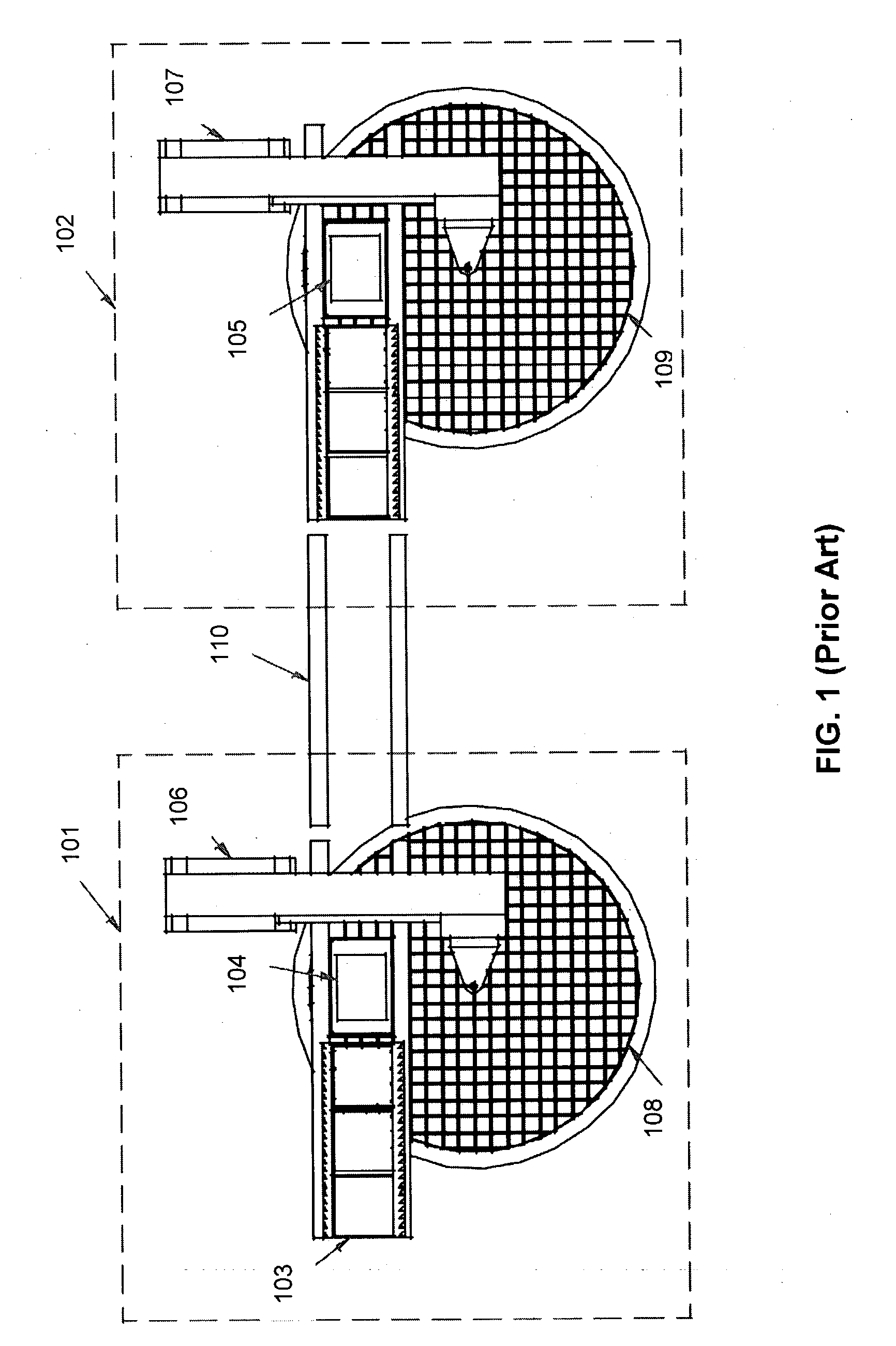
[0014] FIG. 1 is a plan view of a conventional cascade line for a dual bond head die bonding system;

[0015] FIGS. 2a and 2b are plan views of multiple bond-arm systems with a linear arm and a rotary V-arm configuration respectively;

[0016] FIG. 3 is a perspective view of an apparatus according to the preferred embodiment of the invention in the form of a multiple bond head bonding system;

[0017] FIGS. 4a and 4b are plan and front views respectively of the bonding system of FIG. 3 wherein both die delivery devices are at their home positions;

[0018] FIGS. 5a and 5b are plan and front views respectively of the bonding system of FIG. 3 wherein both die delivery devices are at their standby positions;

[0019] FIGS. 6a and 6b are plan and front views respectively of the bonding system of FIG. 3 showing the feed paths of the die holding tools of the die ...


PUM

PropertyMeasurementUnit
timeaaaaaaaaaa
flexibleaaaaaaaaaa
adhesiveaaaaaaaaaa

Abstract

An apparatus is provided for transferring components from a pick-up position amongst a supply of components to a placement position on a receptor, such as a die pad, during semiconductor processing. It includes a first delivery device and a second delivery device operative to alternatively transfer the components from the pick-up position to the placement position. The second delivery device is arranged opposite the first delivery device about a line passing through the pick-up position and the placement position.

Description

[0001] The present invention relates to an apparatus for delivering components or materials such as semiconductor dice or epoxy onto substrates during semiconductor processing, and in particular, to an apparatus with a plurality of delivery devices to execute such operations.BACKGROUND AND PRIOR ART[0002] Pick-and-place machines are commonly used in automated semiconductor equipment to accurately deliver components or materials onto semiconductor substrates, such as leadframes. An example is the die bonding machine, which transfers cut wafer dice or chips from a wafer table onto a substrate in a "pick-and-place" operation. For operational simplicity, single bond head systems are normally used to perform the pick-and-place operation. However, there is a limitation in the throughput (normally quantified in Units Per Hour or "UPH") attainable for single-head systems. Present systems with single bond heads cannot sufficiently fulfill the increasing demand for high throughput, and theref...

Claims


Application Information

Patent Timeline
Patent Type & Authority Applications(United States)
IPC IPC(8): H01L21/67H01L21/00H01L21/52
CPCH01L21/67144Y10T156/1776Y10T156/1092Y10T156/1754Y10T156/1707Y10T156/12Y10T156/1097H01L21/52
Inventor LAM, KUI KAMNG, MAN CHUNG RAYMONDTANG, YEN HSI TERRY
Owner ASM ASSEMBLY AUTOMATION LTD
Why Eureka
Eureka Blog
Learn More