
Memory redundance circuit techniques

a memory redundancy circuit and memory technology, applied in the field of memory devices, can solve the problems of limiting, or even precluding, the scalability of the sram subsystem design, and the specific adaptions of the sram subsystem may fail to obviate,

Inactive Publication Date: 2004-10-07
AVAGO TECH INT SALES PTE LTD
View PDF27 Cites 7 Cited by
  • Summary
  • Abstract
  • Description
  • Claims
  • Application Information

AI Technical Summary

Problems solved by technology

In view of the trends toward compact, high-performance, high-bandwidth integrated computer networks, portable computing, and mobile communications, the aforementioned constraints can impose severe limitations upon memory structure designs, which traditional memory system and subcomponent implementations may fail to obviate.
Furthermore, the SRAM subsystems of many VLSI systems frequently are integrated relative to particular design implementations, with specific adaptions of the SRAM subsystem limiting, or even precluding, the scalability of the SRAM subsystem design.
As a result SRAM memory subsystem designs, even those considered to be "scalable", often fail to meet design limitations once these memory subsystem designs are scaled-up for use in a VLSI system with need for a greater memory cell population and / or density.

Method used


Image

  • Memory redundance circuit techniques
  • Memory redundance circuit techniques
  • Memory redundance circuit techniques

Examples


Embodiment Construction

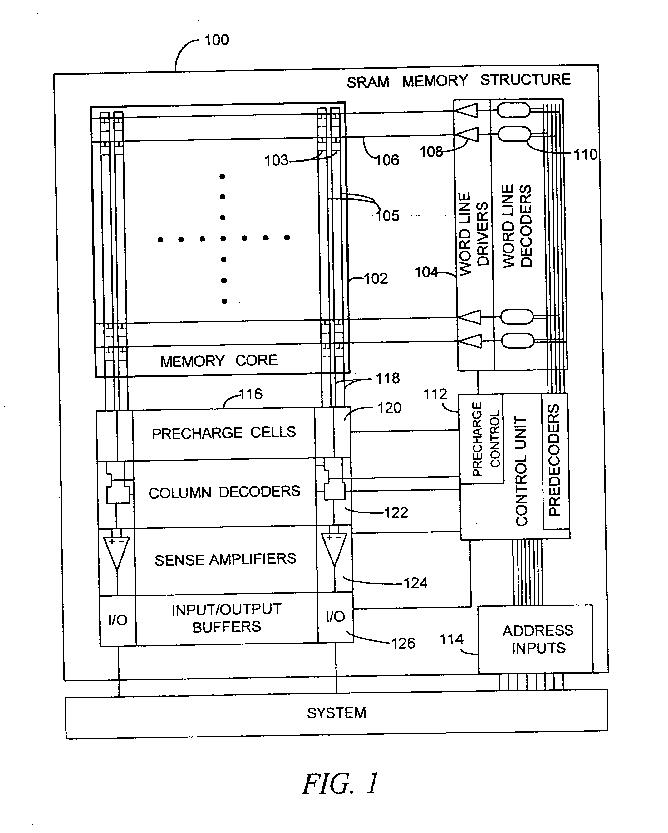
[0050] As will be understood by one having skill in the art, most VLSI systems, including communications systems and DSP devices contain VLSI memory subsystems. Modern applications of VLSI memory subsystems almost invariably demand high efficiency, high performance implementations that magnify the design tradeoff between layout efficient, speed, power consumption, scalability, design tolerances, and the like. The present invention ameliorates these tradeoffs using a novel hierarchical architecture. The memory module of the present invention also can employ one or more novel components which further add to the memory modules efficiency and robustness.

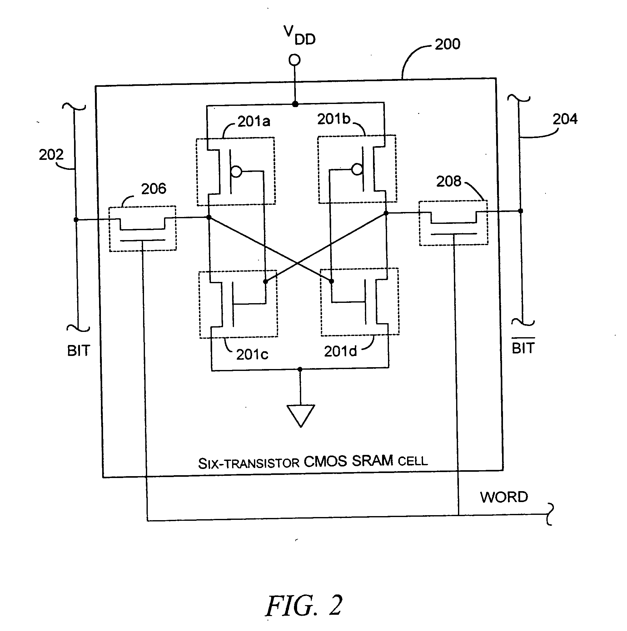
[0051] Hereafter, but solely for the purposes of exposition, it will be useful to describe the various aspects and embodiments of the invention herein in the context of an SRAM memory structure, using CMOS SRAM memory cells. However, it will be appreciated by those skilled in the art the present invention is not limited to CMOS-based pro...


PUM


Abstract

In a memory module having a designated group of memory cells assigned to represent a logical portion of the memory structure, a memory redundancy circuit having a redundant group of memory cells; and a redundancy controller coupled with the designated group and the redundant group. The redundancy controller, which can include a redundancy decoder, assigns the redundant group to the logical portion of the memory structure in response to a preselected memory group condition, e.g., a "FAILED" memory group condition. The redundancy controller also can include selectable switches, for example, fuses, which can encode the preselected memory group condition. The designated group of memory cells and the redundant group of memory cells can be a memory row, a memory column, a preselected portion of a memory module, a selectable portion of a memory module, a memory module, or a combination thereof.

Description

CROSS-REFERENCE TO RELATED APPLICATION(S)[0001] The present application claims the benefit of the filing dates of the following United States Provisional Patent Applications, the contents of all of which are hereby expressly incorporated herein by reference:[0002] Serial No. 60 / 215,741, filed Jun. 29, 2000, and entitled MEMORY MODULE WITH HIERARCHICAL FUNCTIONALITY;[0003] Serial No. 60 / 193,607, filed Mar. 31, 2000, and entitled MEMORY REDUNDANCY IMPLEMENTATION;[0004] Serial No. 60 / 193,606, filed Mar. 31, 2000, and entitled DIFFUSION REPLICA DELAY CIRCUIT;[0005] Serial No. 60 / 179,777, filed Feb. 2, 2000, and entitled SPLIT DUMMY BITLINES FOR FAST, LOW POWER MEMORY;[0006] Serial No. 60 / 193,605, filed Mar. 31, 2000, and entitled A CIRCUIT TECHNIQUE FOR HIGH SPEED LOW POWER DATA TRANSFER BUS;[0007] Serial No. 60 / 179,766, filed Feb. 2, 2000, and entitled FAST DECODER WITH ASYNCHRONOUS RESET;[0008] Serial No. 60 / 220,567, filed Jul. 25, 2000, and entitled FAST DECODER WITH ROW REDUNDANCY;[...

Claims


Application Information

Patent Timeline
Patent Type & Authority Applications(United States)
IPC IPC(8): G11C7/06
CPCG11C5/04G11C7/06G11C29/848
Inventor TERZIOGLU, ESIN
Owner AVAGO TECH INT SALES PTE LTD
Learn More