
System and method for integrating in-situ metrology within a wafer process

Inactive Publication Date: 2004-09-23
LAM RES CORP
View PDF12 Cites 68 Cited by
  • Summary
  • Abstract
  • Description
  • Claims
  • Application Information

AI Technical Summary

Benefits of technology

[0022] The present invention advantageously provides more precise control of the process. The more precise control allows for reduced process time and therefore increased wafer throughput over prior art processes and systems.

Problems solved by technology

If the CMP process is allowed to continue too long then too much overburden material will be removed and the underlying devices can be damaged.
As a result, the circuit formed by the underlying devices would fail to meet the performance goals.
In the alternative, if the CMP process is stopped too early, then an insufficient quantity of the overburden material is removed.
As a result, the remaining overburden material can cause unintended interconnects between the underlying devices.
This is problematic when using wet chemical processes because the film of liquid on the surface of the substrate to be measured complicates and can interfere with the measurement.
Additionally, the typical prior art subsystem or sub-process for monitoring the progress of the respective manufacturing process are inherently inefficient because the process itself must be interrupted and restarted multiple times. Starting and stopping the respective semiconductor manufacturing process can also require additional handling of the semiconductor substrate and a more complex overall semiconductor fabrication process.
The additional handling and more complex process can introduce additional non-uniformities, defects or mistakes in the semiconductor manufacturing process.

Method used


Image

  • System and method for integrating in-situ metrology within a wafer process
  • System and method for integrating in-situ metrology within a wafer process
  • System and method for integrating in-situ metrology within a wafer process

Examples


Embodiment Construction

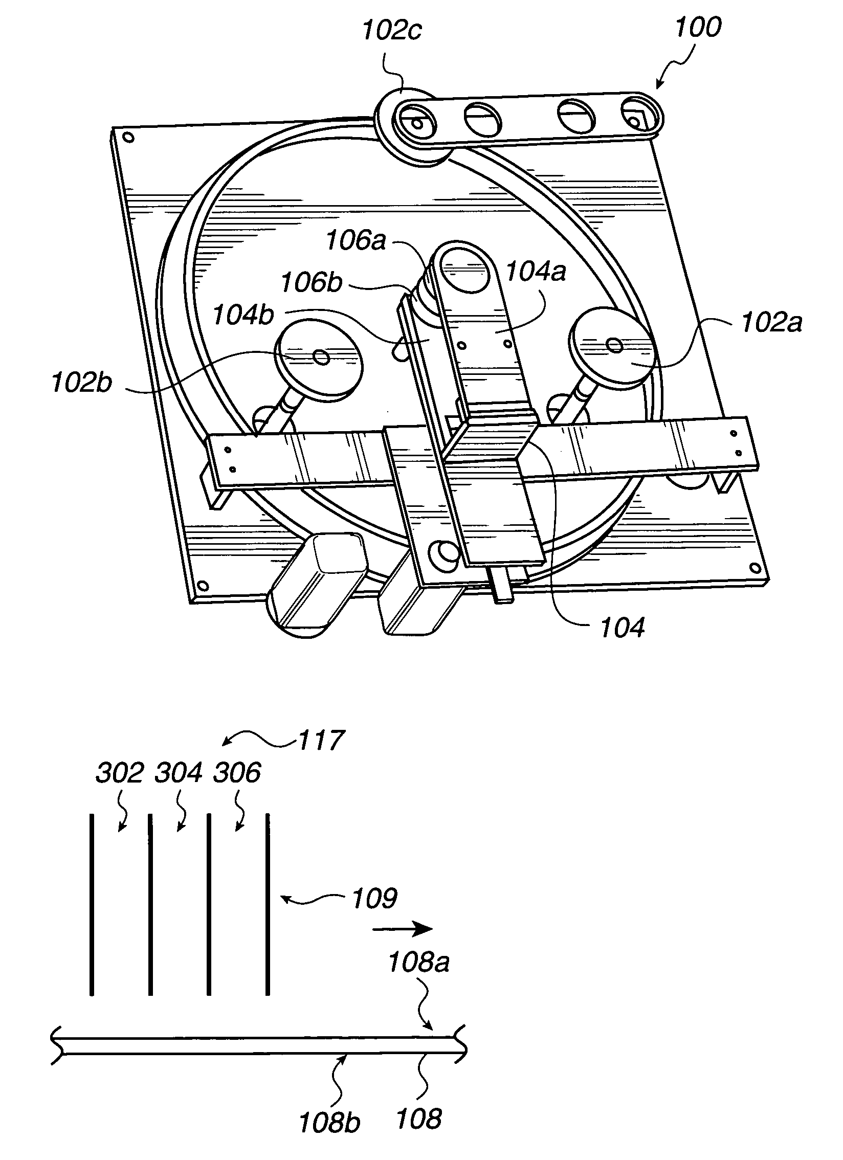
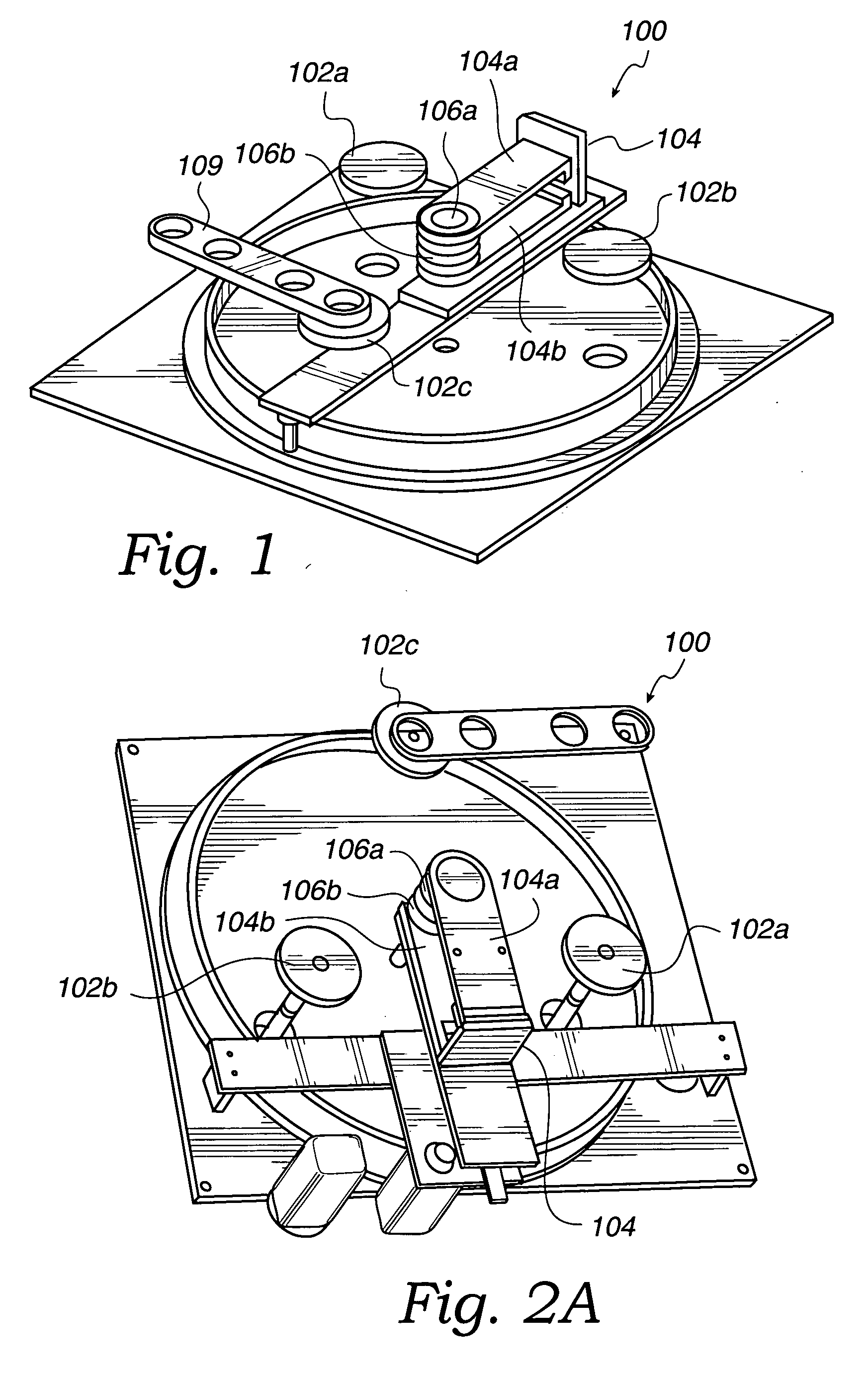
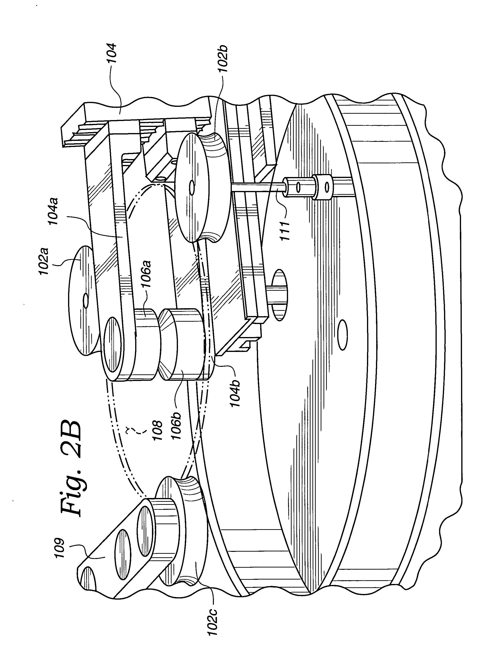
[0061] Several exemplary embodiments for a semiconductor fabrication process that utilizes a surface tension gradient and is combined with an in-situ metrology system will now be described. It will be apparent to those skilled in the art that the present invention may be practiced without some or all of the specific details set forth herein.

[0062] While this invention has been described in terms of several preferred embodiments, it will be appreciated that those skilled in the art upon reading the preceding specifications and studying the drawings will realize various alterations, additions, permutations and equivalents thereof. It is therefore intended that the present invention includes all such alterations, additions, permutations, and equivalents as fall within the true spirit and scope of the invention.

[0063] Semiconductor fabrication processes that utilize a surface tension gradient can be accomplished with a proximity head in one embodiment. Examples of a proximity head are d...


PUM


Abstract

A system and method for processing a wafer includes applying a process to the wafer. The process being supported by a surface tension gradient device. A result of the process is monitored. The monitored result is output.

Description

[0001] This application is a continuation-in-part and claims priority from co-pending U.S. patent application Ser. No. 10 / 330,843 filed on Dec. 24, 2002 and entitled "Meniscus, Vacuum, IPA Vapor, Drying Manifold," which is a continuation-in-part of co-pending U.S. patent application Ser. No. 10 / 261,839 filed on Sep. 30, 2002 and entitled "Method and Apparatus for Drying Semiconductor Wafer Surfaces Using a Plurality of Inlets and Outlets Held in Close Proximity to the Wafer Surfaces." This application is also a continuation in part of U.S. patent application Ser. No. 10 / 330,897, filed on Dec. 24, 2002, entitled "System for Substrate Processing with Meniscus, Vacuum, IPA vapor, Drying Manifold" and is also a continuation in part of U.S. patent application Ser. No. 10 / 404,270, filed on Mar. 31, 2003, entitled "Vertical Proximity Processor," and is also a continuation in part of U.S. patent application Ser. No. 10 / 404,692 filed on Mar. 31, 2003, entitled Methods and Systems for Process...

Claims


Application Information

Patent Timeline
IPC IPC(8): G03F7/20H01L21/00
CPCG03F7/70341H01L21/67028Y10S134/902H01L21/67051H01L21/67034H01L22/00
Inventor BOYD, JOHN M.DE LARIOS, JOHN M.RAVKIN, MICHAELREDEKER, FRED C.
Owner LAM RES CORP
Learn More