Electron microscopy system
- Summary
- Abstract
- Description
- Claims
- Application Information
AI Technical Summary
Benefits of technology
Problems solved by technology
Method used
Image
Examples
Embodiment Construction
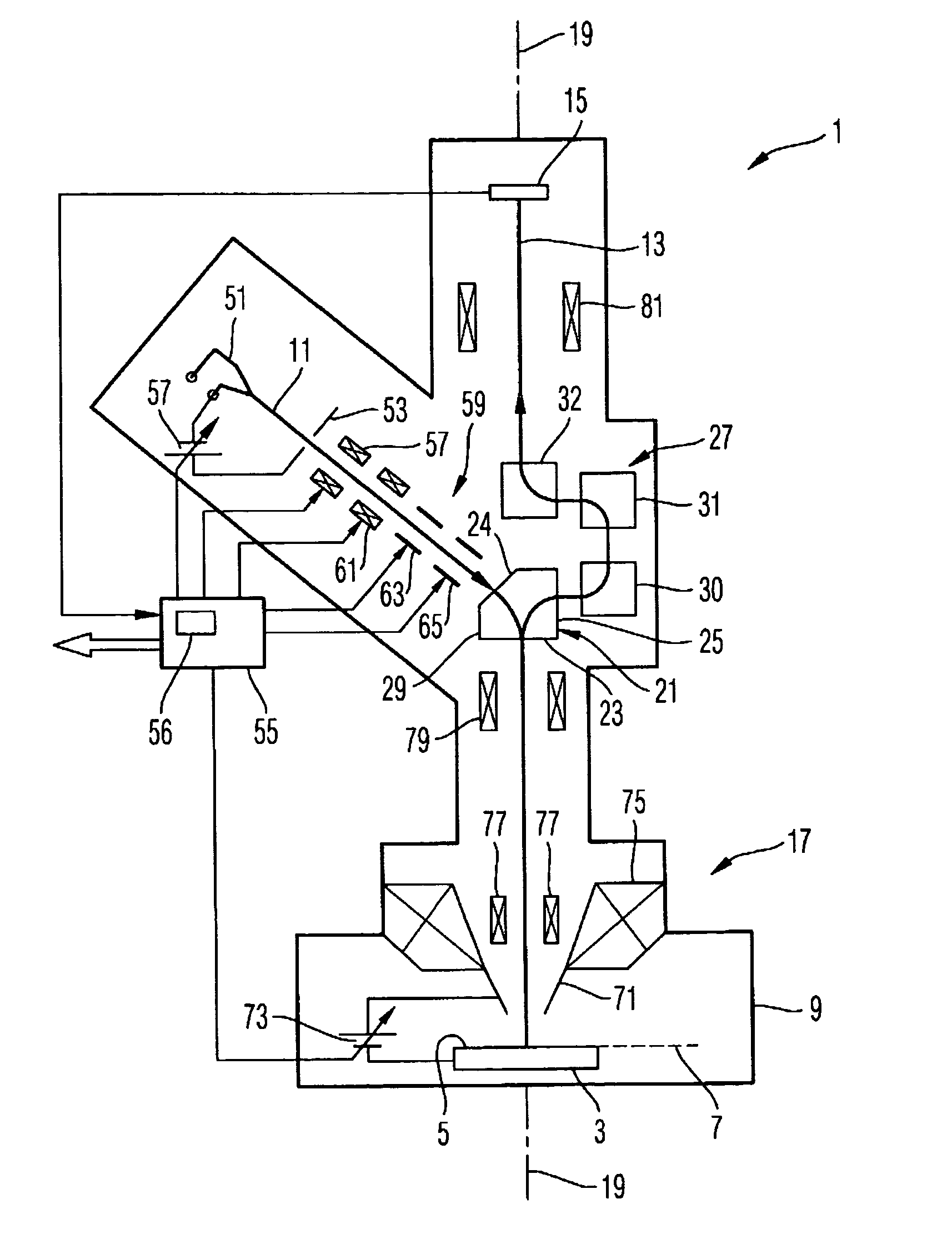
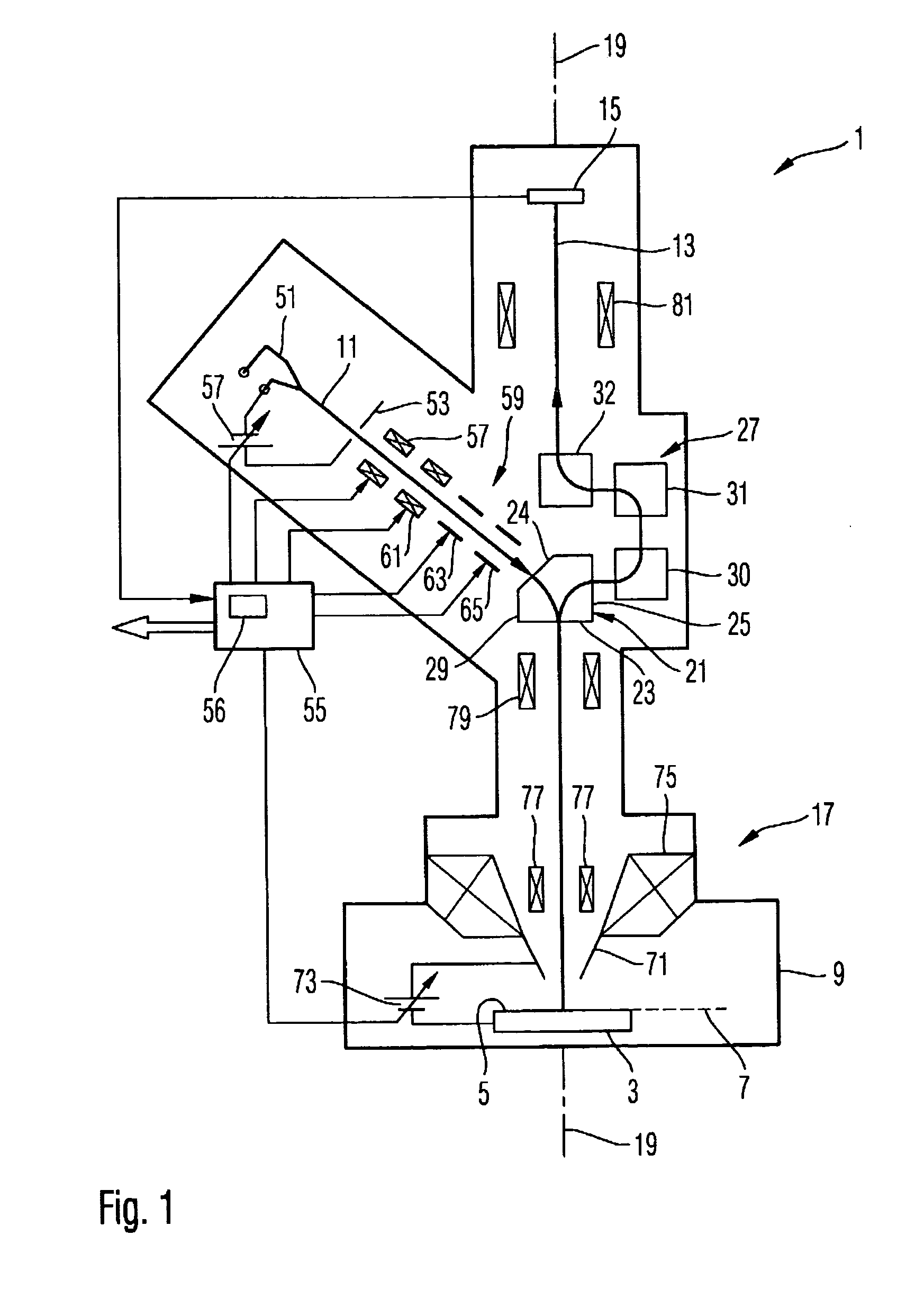
[0031] An electron microscope 1 schematically shown in FIG. 1 serves to generate an electron-microscopic image of an object to be examined, such as a semiconductor wafer 3. A surface 5 of the same is disposed in an object plane 7 of the electron microscope 1 in a sample chamber 9. The electron microscope 1 directs a primary electron beam 11 to the surface 5 of the semiconductor wafer 3, and secondary electrons emanating from a region about the object plane 7 are directed as a secondary electron beam 13 on a detector 15 of the electron microscope 1. The intensities of secondary electrons detected there provide the image information for the image of the object 3 to be generated.
[0032] An objective arrangement 17 is provided, on the one hand, for directing the primary electron beam 11 to the surface 5 of the wafer 3 and, on the other hand, for collecting the secondary electrons emerging from the wafer 3 and for shaping the same to the secondary electron beam 13. The objective arrangeme...
PUM
 Abstract
Description
Claims
Application Information
 - R&D
- Intellectual Property
- Life Sciences
- Materials
- Tech Scout
- Unparalleled Data Quality
- Higher Quality Content
- 60% Fewer Hallucinations
Browse by: Latest US Patents, China's latest patents, Technical Efficacy Thesaurus, Application Domain, Technology Topic, Popular Technical Reports.
© 2025 PatSnap. All rights reserved.Legal|Privacy policy|Modern Slavery Act Transparency Statement|Sitemap|About US| Contact US: help@patsnap.com


