Light emitting device and method of manufacturing the same

a technology of light emitting device and manufacturing method, which is applied in the direction of semiconductor devices, basic electric elements, electrical apparatus, etc., can solve the problems of deterioration phenomenon, reduced light emitting intensity, and structural defect, and achieve the effect of reducing the intensity of light emitting with the passage of tim

Inactive Publication Date: 2004-04-22
SEMICON ENERGY LAB CO LTD
View PDF11 Cites 35 Cited by
  • Summary
  • Abstract
  • Description
  • Claims
  • Application Information

AI Technical Summary

Problems solved by technology

Although a liquid crystal display device is used as an image display means in various electronic devices, it has a structural defect such as a narrow view angle.
On the other hand, there are various deterioration phenomena with respect to the organic light emitting element and thus these are regarded as problems.
In particular, when the organic light emitting element is driven for a long time, there is a deterioration phenomenon such that a light emitting intensity decreases with the passage of time.
Thus, this becomes a large hindrance to practical use.
However, even if such a sealing structure is used, the deterioration of the organic light emitting element cannot be completely prevented under the current state.
Generally, an excitation process from a triplet to a singlet is a forbidden transition (spin forbidden transition) and thus is hard to produce.
As a result, it is expected that an electron transport characteristic is deteriorated.
However, it can be explained that impurities such as oxygen and moisture, which are included in the organic compound, cause various deterioration phenomena such as intensity reduction.
If the stress is large, a crack is caused.
However, even if such a treatment is performed, moisture and oxygen in the closed space cannot be completely removed.
As a result, even if complete sealing is performed, the deterioration of the organic light emitting element cannot be prevented.
Thus, the temperature cycle processing after that is not particularly performed.
However, thermal treatment is not performed during these processes.
However, repetition of atmosphere exposure is not an effective method.
If the second electrode has a defect and thus a defect is caused in the pixel portion, there is a possibility that it is recognized as a line defect.

Method used


Image

  • Light emitting device and method of manufacturing the same
  • Light emitting device and method of manufacturing the same
  • Light emitting device and method of manufacturing the same

Examples


embodiment 2

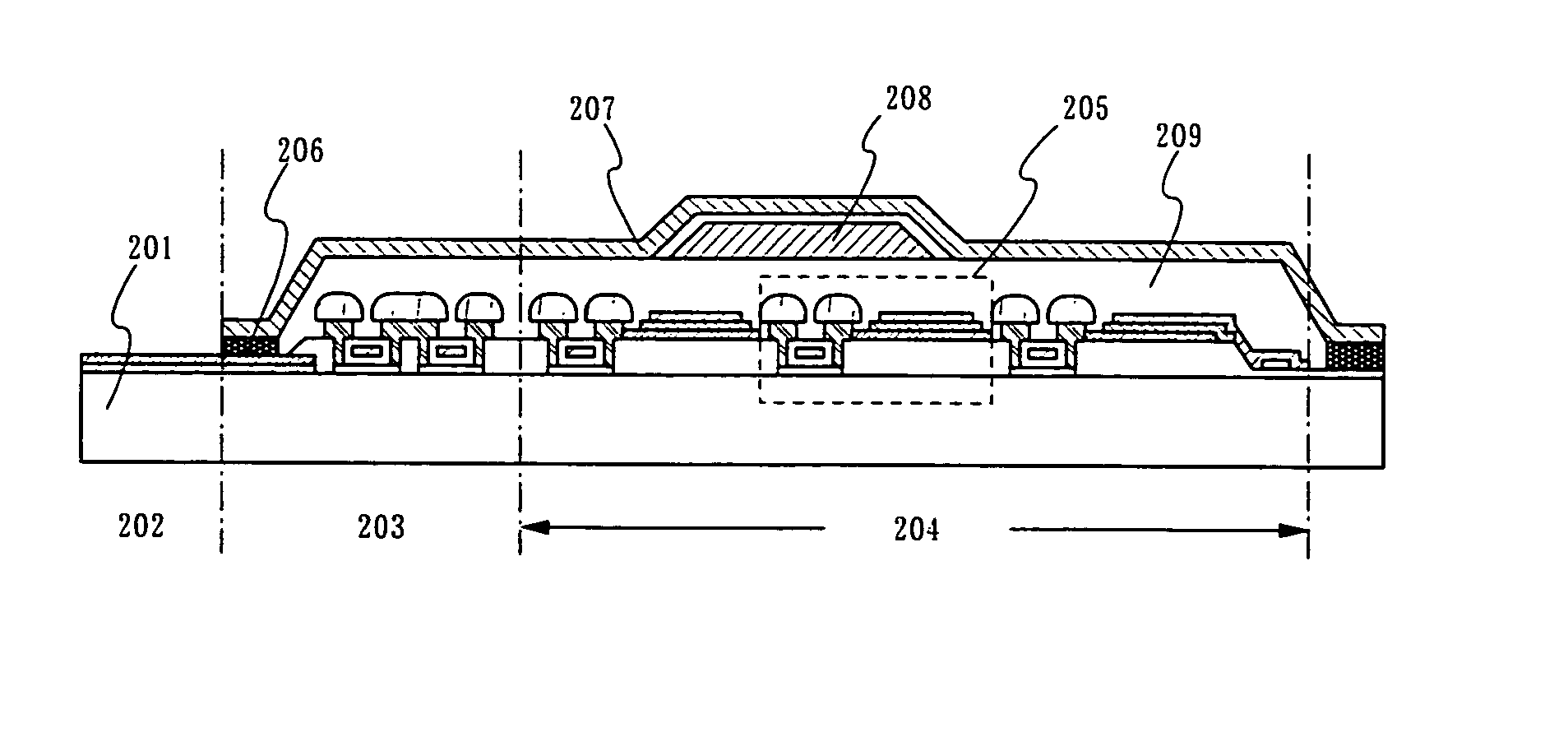
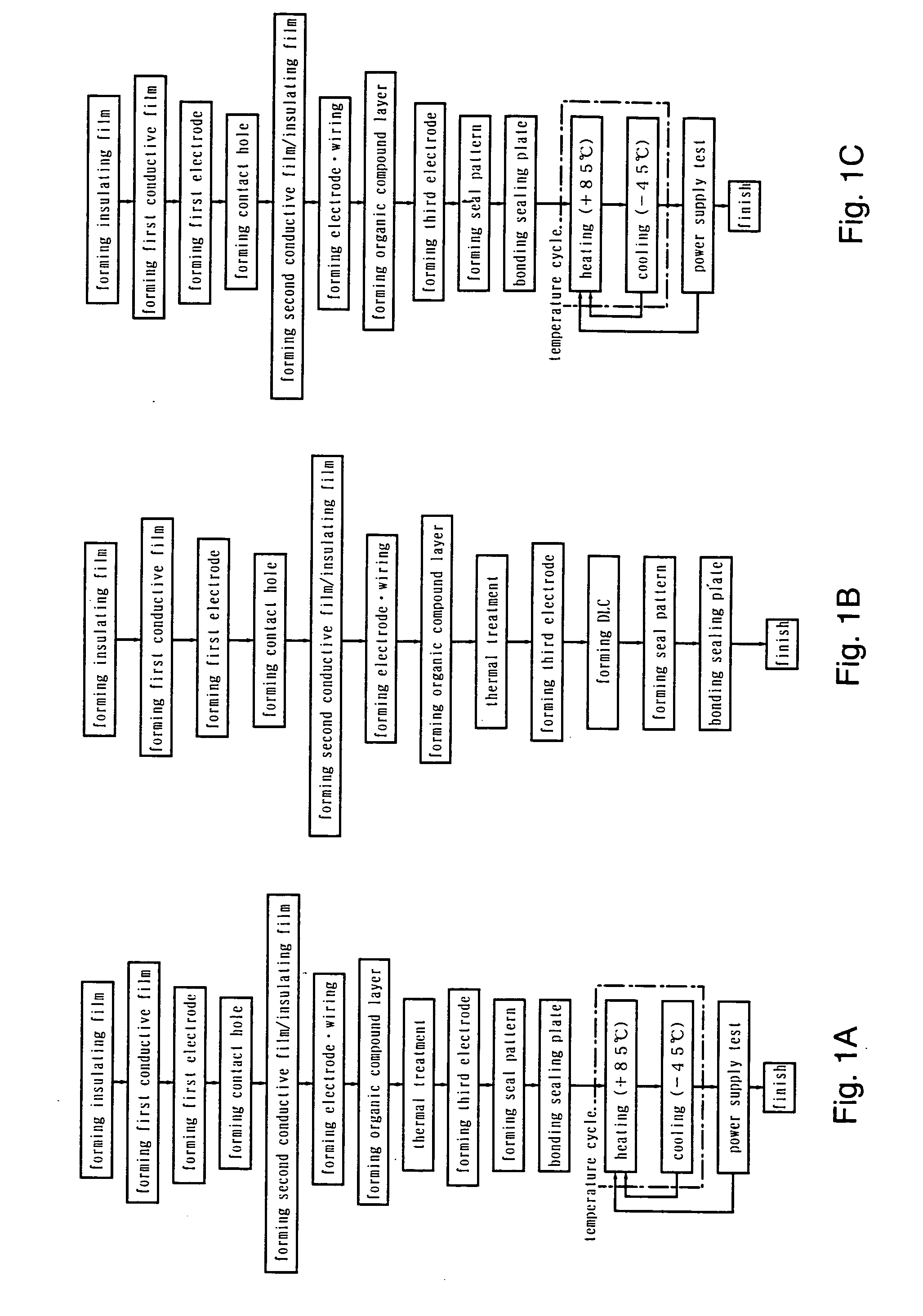
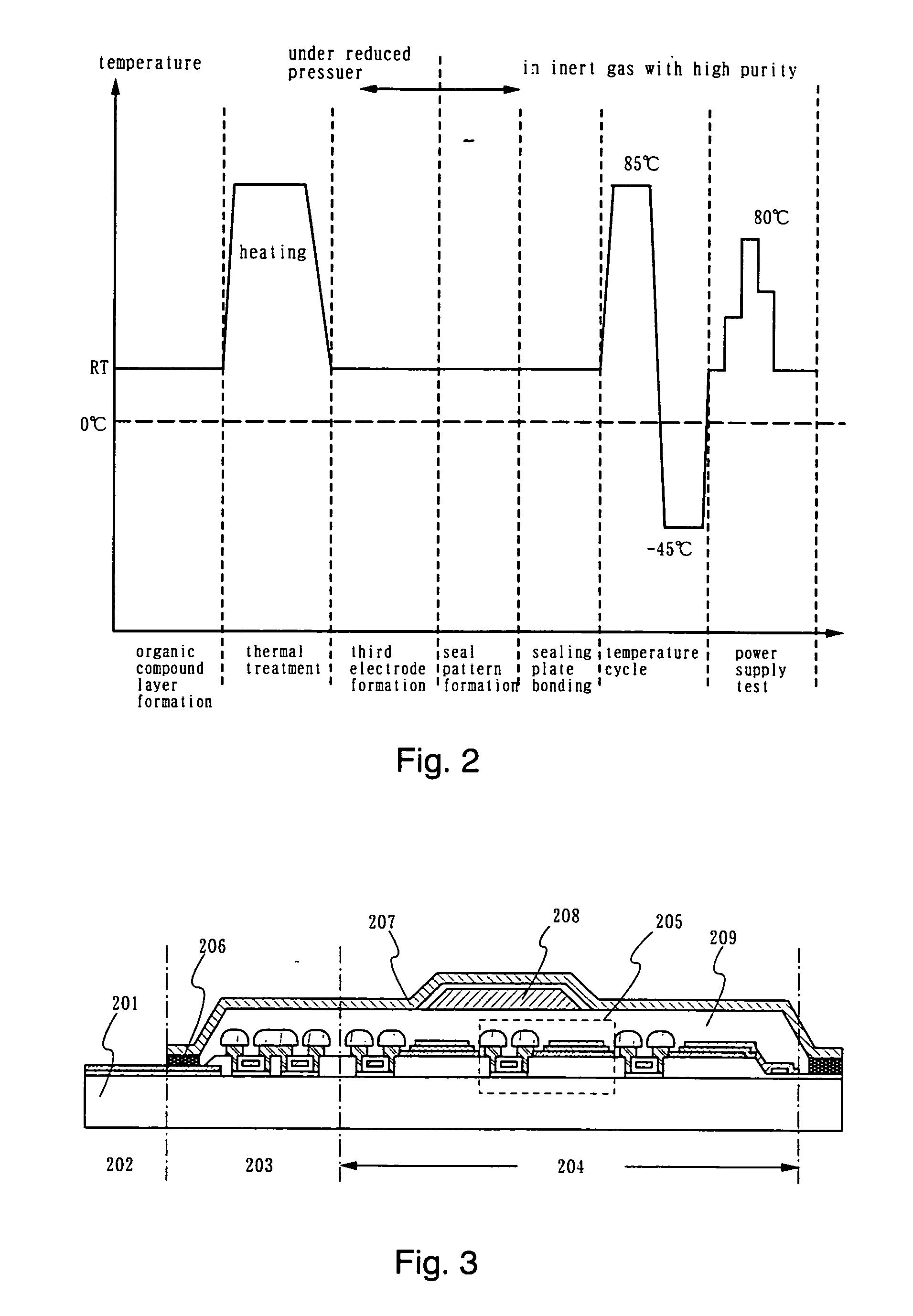
[0098] Another structure of the organic light emitting element described using FIGS. 8A to 8C in Embodiment 1 will be described with reference to FIG. 9. A seventh insulating film is formed after the formation of the anode 411. This insulating film is made of silicon oxide or silicon nitride. After that, the seventh insulating film located on the anode 411 is removed by etching. At this time, as shown in FIG. 9, end portions of the anode 411 is overlapped with the seventh insulating film. Thus, a pattern-formed seventh insulating film 440 is obtained.

[0099] Later processes are performed as in the case of Embodiment 1 to form the connection electrode 415, the insulating film 419, and the like. The organic compound layer 424 and the cathode 425 are formed as shown in FIG. 9. When the seventh insulating film 440 is provided, it can be prevented that the cathode 425 is in contact with the anode 411 in the end portions and a short circuit is caused.

[0100] Of course, even in the case of t...

embodiment 3

[0101] One example of a top gate TFT is described in Embodiment 1. However, even when a bottom gate TFT or an inverse stagger TFT is used, the switching TFT 430 and the current control TFT 432 can be formed as in the case of Embodiment 1. In addition, the light emitting device can be manufactured as in the case of Embodiment 1.

embodiment 4

[0102] With respect to the organic light emitting element applied in the present invention, there is no case where its structure is limited. The organic light emitting element is composed of an anode made from a translucent conductive film, a cathode including alkali metal, and a layer made of an organic compound, which is interposed therebetween. The layer made of an organic compound composed of a single layer or plural layers. The respective layers are separately called a hole injection layer, a hole transport layer, a light emitting layer, an electron transport layer, an electron injection layer, and the like in accordance with their purposes and functions. These layers can be formed by a small molecular system organic compound material, a polymer system organic compound material, or a suitable combination of both materials.

[0103] For the hole injection layer and the hole transport layer, an organic compound material having superior hole transport characteristic is selected. Typi...


PUM


Abstract

Two aspects, an impurity factor and a structural factor are assumed as the deterioration causes of an organic light emitting device and means for solving the respective factors are provided. In order to prevent deterioration of the light emitting device, concentrations of moisture and oxygen, which are left in a space in which an organic light emitting element is sealed, are minimized. At the same time, an impurity including oxygen, such as moisture or oxygen which is included in an organic compound composing the organic light emitting element, is reduced. An element structure for preventing the deterioration of the organic light emitting element due to stress is used to suppress the deterioration.

Description

[0001] 1. Field of the Invention[0002] The present invention relates to a light emitting device using a phosphor or a light emitting element and a method of manufacturing the same. More particularly, the present invention relates to a light emitting device manufactured using an organic compound for a phosphor or a light emitting element and a method of manufacturing the same. Note that light emission in this specification includes fluorescence and phosphorescence and that the present invention includes light emission by any one of them or both.[0003] 2. Description of the Related Art[0004] In a typical display device using liquid crystal, a back light is used and it is constructed such that an image is displayed by the back light. Although a liquid crystal display device is used as an image display means in various electronic devices, it has a structural defect such as a narrow view angle. On the other hand, since a display device using a phosphor for a pixel portion has a wide view...

Claims


Application Information

Patent Timeline
Patent Type & Authority Applications(United States)
IPC IPC(8): H01L27/12H01L27/32H01L51/52
CPCH01L27/12H01L27/3244H01L27/3246H01L51/5259H01L27/3281H01L51/5203H01L51/5237H01L27/3276H10K59/17H10K59/122H10K59/12H10K59/131H10K50/841H10K50/846H10K50/844H10K59/805H10K50/805
Inventor YAMAZAKI, SHUNPEIMIZUKAMI, MAYUMIARAI, YASUYUKI
Owner SEMICON ENERGY LAB CO LTD
Why Eureka
Try Eureka