Copper plating solution for embedding fine wiring, and copper plating method using the same

a technology of fine wiring and copper plating solution, which is applied in the direction of basic electric elements, electrical equipment, semiconductor devices, etc., can solve the problems that the copper plating solution may not be uniformly plated with the copper sulfate solution, and the copper plating solution is not suitable for filling the fine gaps between the wiring patterns. , defects, voids and seams

Inactive Publication Date: 2003-05-08
ELECTROPLATING ENGINEERS OF JAPAN LTD
View PDF5 Cites 49 Cited by
  • Summary
  • Abstract
  • Description
  • Claims
  • Application Information

AI Technical Summary

Problems solved by technology

However, it has been pointed out that use of the additive-containing plating solution of copper sulfate may cause the following problems.
The wafer coated with the copper seed film may not be uniformly plated with the copper sulfate solution, because the solution tends to dissolve the copper seed film.
More specifically, filling the fine gaps between the wiring patterns with the copper plating solution may produce defects, e.g., voids and seams, in the gaps.
However, the plating solution of unbalanced composition will be less stable than the common plating solution of copper sulfate, and deteriorate uniformity of the copper plating treatment, because it tends to decompose the additive used for controlling electrodeposition.
As a result, it is difficult to continuously keep the uniform copper plating.
Viewed from its relationship with concentration of copper sulfate (more specifically copper), however, it satisfies the unbalanced composition of high-concentration copper sulfate and low-concentration sulfuric acid.
A sulfuric acid concentration below 5 g / L is accompanied by decreased current efficiency, and difficulty in the uniform plating treatment.
Moreover, the plating solution declines in capacity to fill the gaps between the fine wiring patterns at a chlorine concentration beyond 20 to 200 mg / L, tending to leave voids in the plated gaps.
At above 20 g / L, on the other hand, it may excessively control the reaction, with the result that the reaction may not proceed uniformly, tending to produce seams in the fine gaps.
The one having a molecular weight of less than 100 may not be effective because of the insufficient capacity of controlling the electrodeposition reaction.
At above 100 mg / L, on the other hand, it will start accelerating the reaction in the area other than the fine gap inside, tending to produce voids in the gaps, and the uniform copper plating treatment may not be realized.
On the other hand, the one having an average molecular weight above 100,000 tends to make the plating treatment for embedding wiring unstable, conceivably resulting from uneven adsorption of the compound.
The macromolecular amine compound having an average molecular weight of 5,000 to 100,000 is difficult to diffuse into the gaps between fine wiring patterns, preventing to a lesser extent the function of the sulfur-based saturated organic compound for accelerating the electrodeposition reaction.
However, it will not contribute much to the improved uniformity, unless its content is increased to some extent, when it has a relatively high average molecular weight (10,000 to 100,000).
It is difficult to fully exhibit its function of leveling thickness of the deposited copper at below 0.01 mg / L.
At above 10 mg / L, on the other hand, it may excessively exhibit the leveling effect to prevent the effect of the sulfur-based saturated organic compound for accelerating the electrodeposition reaction and to cause the conformal separation in which the deposited copper is deposited in the gaps between fine wiring patterns to the same thickness as is on the surface side, with the result that seams and voids tend to be formed in the gaps.
The sulfur-based saturated organic compound is decomposed significantly, especially in the plating solution having a composition of high-concentration copper and low-concentration sulfuric acid, to reduce serviceability of the solution.
It will have an insufficient function of preventing decomposition of the sulfur-based saturated organic compound to cause deterioration of the plating solution, when contained at below 0.025 g / L.
At above 25 g / L, on the other hand, it may cause self-decomposition of the plating solution, conversely tending to make the solution unstable.
It may not fully exhibit its leveling function at below 0.01 mg / L, deteriorating the final appearances of the plated product.
At above 20 mg / L, on the other hand, it may not effectively fill the gap insides with copper.

Method used


Image

  • Copper plating solution for embedding fine wiring, and copper plating method using the same
  • Copper plating solution for embedding fine wiring, and copper plating method using the same
  • Copper plating solution for embedding fine wiring, and copper plating method using the same

Examples


Embodiment Construction

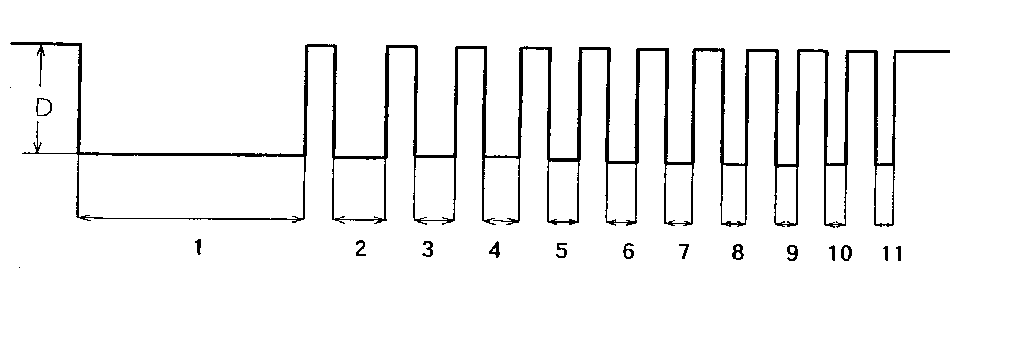
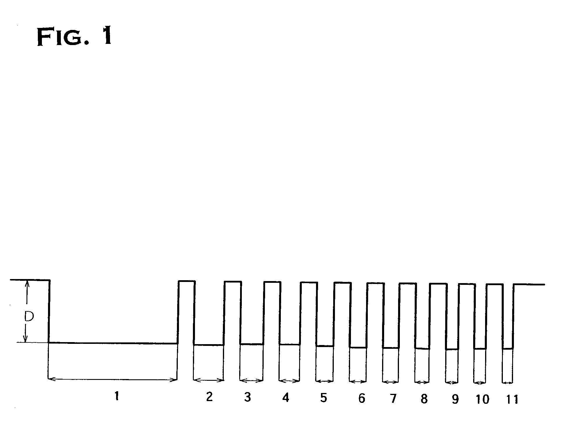
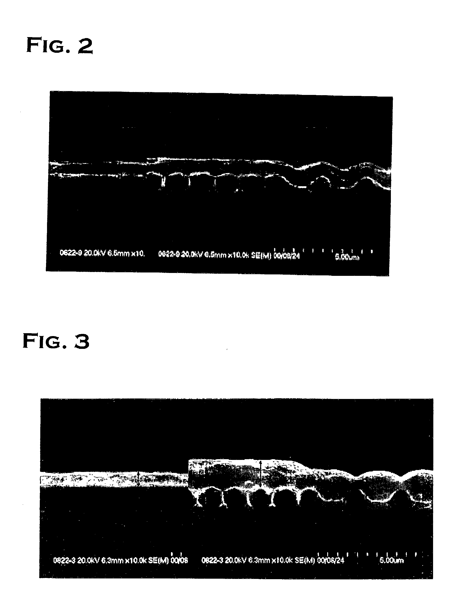
1.0 20 0.01 2.5 0.5 0.55 .largecircle. .largecircle. Example 2 1.0 20 0.1 2.5 0.5 0.05 .largecircle. .largecircle. Example 3 1.0 20 1.0 2.5 0.5 0.07 .largecircle. .largecircle. Example 4 1.0 20 10.0 2.5 0.5 0.05 .DELTA. .DELTA. Example 5 1.0 20 20 2.5 0.5 0.06 X X Example 6 1.0 20 0.1 0.025 0.5 0.05 .largecircle. .DELTA. Example 7 1.0 20 0.1 2.5 0.5 0.06 .largecircle. .largecircle. Example 8 1.0 20 0.1 5.0 0.5 0.06 .largecircle. .largecircle. Example 9 1.0 20 0.1 25 0.5 0.05 .DELTA. .DELTA. Example 10 1.0 20 0.1 30 0.5 0.05 X X Example 11 1.0 20 10.0 2.5 0.5 0.05 .largecircle. .largecircle. Comparative 1.0 20 -- -- 0.5 0.74 X X Example 1 Comparative 1.0 20 -- 2.5 0.5 0.79 .largecircle. .largecircle. Example 2 Comparative 1.0 20 0.1 -- 0.5 0.06 .DELTA. X Example 3

[0043]

2TABLE 2 A Concentration [g / L] of a macromolecular, triol type surfactant of polypropylene glycol (PPG) having an average molecular weight of 5,000 B Concentration [mg / L] of 3,3-dithiobis-propane-sodium sulfonate C Con...


PUM

PropertyMeasurementUnit
Densityaaaaaaaaaa
Densityaaaaaaaaaa
Densityaaaaaaaaaa

Abstract

The present invention provides a copper plating solution for embedding fine wiring, wherein it contains copper sulfate at 100 to 300 g / L as copper sulfate pentahydrate, sulfuric acid at 5 to 300 g / L, chlorine at 20 to 200 mg / L, a macromolecular surfactant at 0.05 to 20 g / L for controlling the electrodeposition reaction, sulfur-based saturated organic compound at 1 to 100 mg / L for accelerating the electrodeposition reaction, leveling agent composed of a macromolecular amine compound at 0.01 to 10 mg / L and reductant at 0.025 to 25 g / L for stabilizing the copper plating solution. The copper plating solution of the present invention for embedding fine wiring can plate the wafer surface provided with fine wiring patterns with sub-micron order gaps in-between and coated with copper serving as the metallic seed film, to fill the gaps neither leaving any defect therein nor dissolving the metallic seed film.

Description

[0001] 1. Field of the Invention[0002] The present invention relates to a plating treatment technique for the surface of a wafer as an electronic device, more particularly to a plating solution of copper sulfate for embedding copper by plating on the wafer surface on which fine wiring patterns with sub-micron order gaps in-between are formed.[0003] 2. Description of the Related Art[0004] Recently, the fine processing techniques for a wafer as an electronic device have made rapid progress, and the plating techniques for processing wafers have been also extensively under development. The plating techniques for processing wafers include copper plating based on electrolysis, and the representative electrolytic plating solution includes strongly acidic solutions of copper sulfate, and alkaline solutions of cyan- and pyrophosphoric acid-based ones. Among these plating solutions, a strongly acidic solution of copper sulfate has been widely used, because it can be more easily managed and co...

Claims


Application Information

Patent Timeline
IPC IPC(8): C25D3/38C25D7/12H01L21/28H01L21/288
CPCC25D3/38
Inventor TOTSUKA, TAKASHIKUZUSHIMA, TOSHIO
Owner ELECTROPLATING ENGINEERS OF JAPAN LTD
Why Eureka
Try Eureka