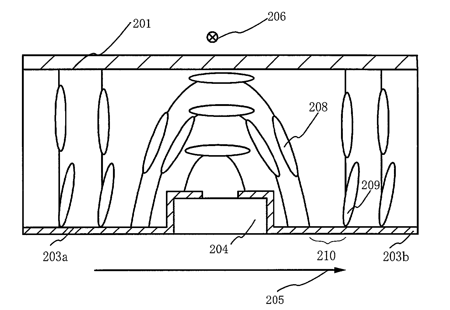
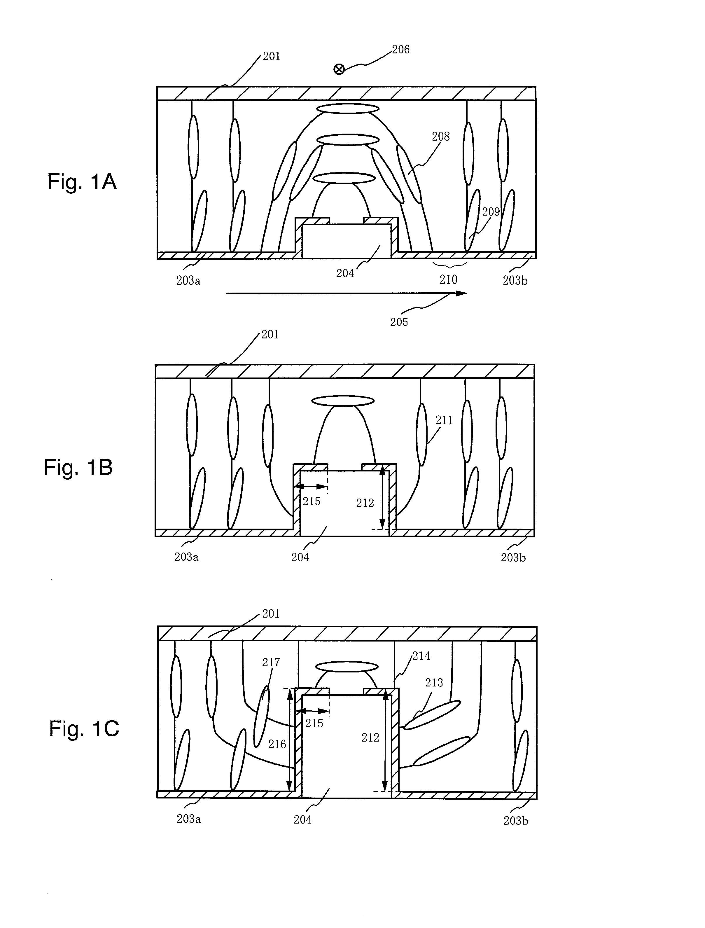
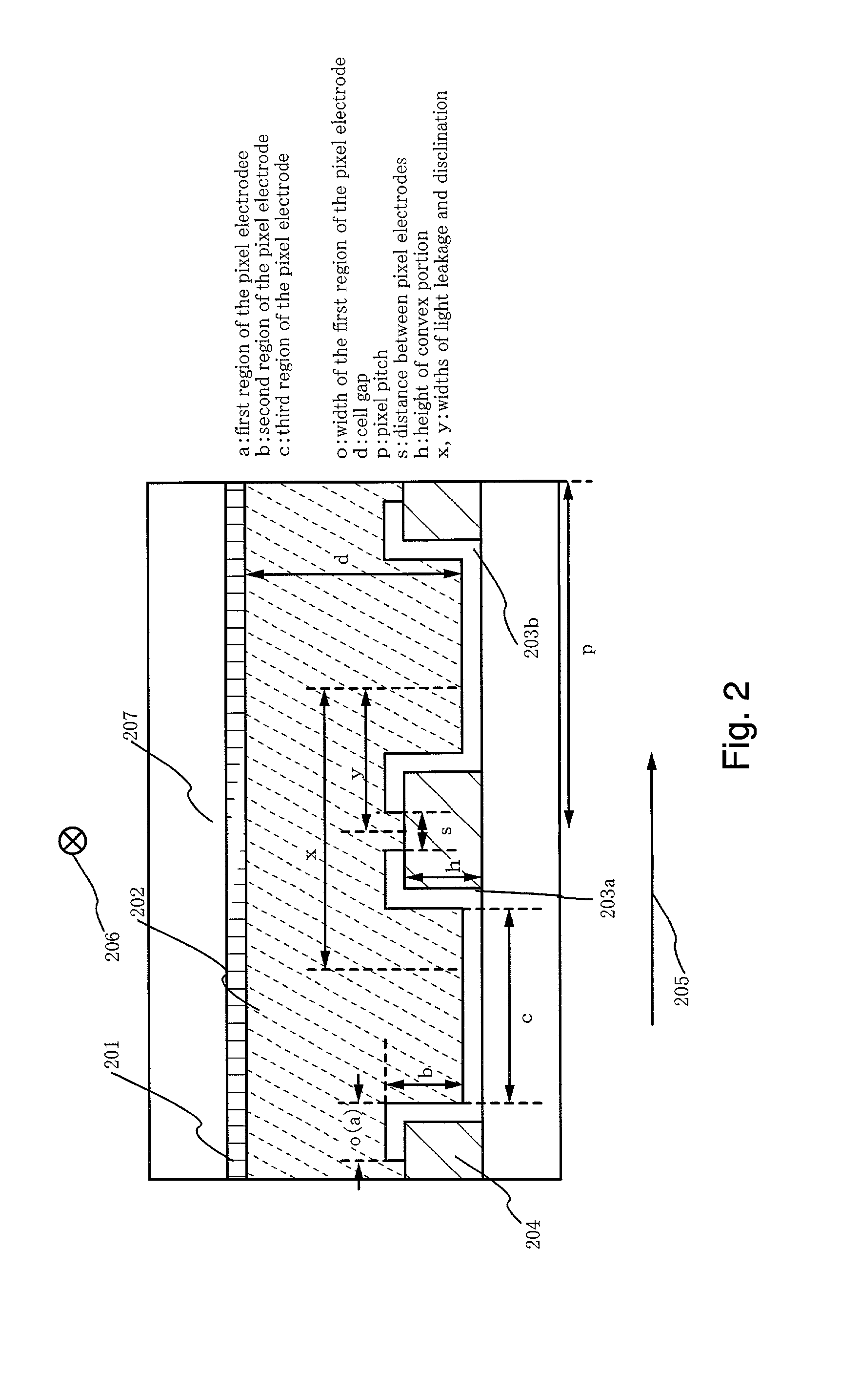
Liquid crystal display device
a liquid crystal display and display device technology, applied in non-linear optics, instruments, optics, etc., can solve problems such as rubbing irregularities, dislocation and light leakage,
- Summary
- Abstract
- Description
- Claims
- Application Information
AI Technical Summary
Problems solved by technology
Method used
Image

Examples
embodiment 1
[0162] [Embodiment 1]
[0163] An embodiment of the present invention is explained using FIGS. 21A to 25.
[0164] Note that a description is set forth regarding a step for fabricating a pixel TFT; a switching element of the pixel portion and TFTs for driver circuit (a signal line driver circuit and a scanning line driver circuit) provided in the pixel portion of a display device using the driver method of the present invention and periphery portion of the pixel portion. For the simplicity of the explanation, a CMOS circuit, which is a fundamental structure circuit for the driver circuit portion, and the n-channel TFT for the pixel TFT of the pixel portion are shown in figures by a cross-sectional figure according to the path.
[0165] First, as shown in FIG. 21A, a base film 401 made of an insulating film such as a silicon oxide film, a silicon nitride film, or a silicon oxynitride film, is formed on a substrate 400 made of a glass such as barium borosilicate glass or aluminum borosilicate ...
embodiment 2
[0197] [Embodiment 2]
[0198] A portion of the method of manufacturing the active matrix substrate manufactured by Embodiment 1 can be applied to a reflection type liquid crystal display device.
[0199] Processing is first performed in accordance with FIGS. 21A to 22C of Embodiment 1.
[0200] The first interlayer insulating film 472 is then formed from a silicon oxynitride film having a thickness of 100 to 200 nm, as shown in FIG. 27. An acrylic resin film or a polyimide film is then formed with a thickness of 1.8 .mu.m on the first interlayer insulating film 472 as the second interlayer insulating film 473. An etching process is performed next in order to form contact holes.
[0201] Next, as shown in FIG. 28, a photolithography process is performed using a photosensitive resin film, and the convex portion 600 is formed having a thickness of 0.32 .mu.m on the source wiring 483. A material in which JSR Corporation product BPR-107VL is diluted by PGMEA (propylene glycol monomethyl ether aceta...
embodiment 3
[0212] [Embodiment 3]
[0213] In this embodiment, the manufacturing process of an active matrix liquid crystal display device from the active matrix substrate manufactured in Embodiment 1 is described below. FIG. 26 is used for explanation.
[0214] First, in accordance with Embodiment 1, the active matrix substrate is obtained. FIG. 26 shows a cross-sectional view taken along the line A-A' and C-C' of the pixel portion of the active matrix substrate shown in FIG. 25. In an active matrix substrate, the driver circuit portion 506 and the pixel portion 507 are formed.
[0215] First, an orientation film 512 is formed on the active matrix substrate, and is subjected to a rubbing process. Note that, in this embodiment, before the formation of the orientation film 512, a columnar spacer for maintaining a gap between the substrates is formed at a desired position by patterning an organic resin film such as an acrylic resin film. The columnar spacer having 4.0 .mu.m height is used in this embodime...
PUM
 Abstract
Description
Claims
Application Information
 - R&D
- Intellectual Property
- Life Sciences
- Materials
- Tech Scout
- Unparalleled Data Quality
- Higher Quality Content
- 60% Fewer Hallucinations
Browse by: Latest US Patents, China's latest patents, Technical Efficacy Thesaurus, Application Domain, Technology Topic, Popular Technical Reports.
© 2025 PatSnap. All rights reserved.Legal|Privacy policy|Modern Slavery Act Transparency Statement|Sitemap|About US| Contact US: help@patsnap.com