
Interface circuit device for performing data sampling at optimum strobe timing

a technology of data sampling and interface circuit, applied in the direction of generating/distributing signals, instruments, sustainable buildings, etc., can solve the problems of increasing the cost of memory units, affecting the accuracy of data sampling, and reducing the flexibility of design

Inactive Publication Date: 2001-08-16
RENESAS ELECTRONICS CORP
View PDF5 Cites 86 Cited by
  • Summary
  • Abstract
  • Description
  • Claims
  • Application Information

AI Technical Summary

Problems solved by technology

For ensuring such small specification values of the short set-up time and hold time, it is necessary to determine whether the specification values are accurately satisfied or not, and an expensive tester is required for such determination, resulting in increased cost of the memory unit.
Therefore, a system designer cannot freely determine the transfer rate and the data bus width so that flexibility in design is considerably low.
Due to such less timing margin, it may be impossible to take in accurate data in many cases.
Therefore, as shown in FIG. 79, failures occur in the set-up margin and the hold margin for data when variations in propagation delay occur among the memory units in data transfer.
For matching the impedances of the on-board wiring lines with each other, if wiring lines of equal lengths may be arranged between the memory units and the memory controller, the board must have a multi-layered structure, and the wiring must be made in a three-dimensional structure so that the circuit-board becomes expensive.
Thus, the timing margin for taking in the data becomes inadequate, and the memory system capable of accurate data transfer cannot be achieved.
Therefore, it is extremely difficult to make a propagation delay on a signal transfer path, which extends from the clock generator through the memory module, data line and input pad to the register (receiver) of the controller, equal for all the memory modules (memory chips).
Accordingly, it is difficult to achieve the on-board memory system, in which fast and accurate data transfer can be achieved under fast operation environments.
However, provision of such DLL in memory unit MU increases the chip area of memory unit MU as well as power consumption, and in addition, the memory unit becomes expensive due to increase in chip area.
The following problems arise if the margin for data take-in timing at the memory controller changes in accordance with the position / number of the chips or modules in an on-board system.
Specifically, if an error occurs in the data taken by the memory controller, it is difficult to determine whether the cause of this error is present in the data transfer path itself or in the memory unit (or chip).
Thus, it is difficult to detect and eliminate the cause of error at the board level.
When data transfer is performed using a fast clock signal close to, e.g., 1 GHz in such on-board multi-processor system, margins of the set-up time and hold time for data sampling become extremely small and data cannot be transferred fast and accurately, resulting in a problem similar to that of the memory system already described above.
A similar problem occurs in a multiprocessor system, in which a plurality of processors are coupled in parallel to a common data bus, and access a common memory without control of a memory controller.
Particularly, in the case where the system is expanded so that the number of processors increases or an impedance of the data bus increases, a skew of data with respect to a clock signal changes to impair the reliability of the system, resulting in low expandability of the system.
Therefore, fast rising of the data bits may become impossible.
The position of the trailing edge of the effective data window is not corrected because a speed-down occurs in the changing speed of the leading edge according to this push-out.
If this memory device operates accurately, it is determined that the cause of faulty is present in the data bus on the board.
In this case, erroneous determination of data "0" and "1" may occur.
However, even such a memory system can be used for an application where a large amount of data is used, and partial error in determination of data "0" and "1" exerts only a small influence, such as graphic data.
In the case of system expansion, therefore, a large deviation occurs in data strobe timing, resulting in a problem that the system expandability is low.
When a data quality failure is detected, it is merely required to execute the system reset.

Method used


Image

  • Interface circuit device for performing data sampling at optimum strobe timing
  • Interface circuit device for performing data sampling at optimum strobe timing
  • Interface circuit device for performing data sampling at optimum strobe timing

Examples


Embodiment Construction

[0353] Description has been given on the memory devices that perform the data transfer at the double data rate (DDR) mode. However, the memory device employed in the present invention may be a device, which in turn transfers the data in synchronization with one of the rising and falling edges of the clock signal, or in an EDO mode. Further, the memory device may be a flash memory.

[0354] According to the present invention, as described above, the data window is detected from the data on the data line for optimizing the data strobe timing, and therefore the data transfer can be performed accurately regardless of the system structure. In the case of a memory system, a DLL for producing a data outputting clock is not required, and therefore the chip area and the power consumption can be reduced. Further, the data window width is monitored on a data receiving side, so that transfer of erroneous data can be prevented, and the reliability of the system can be ensured.

[0355] Although the pr...


PUM


Abstract

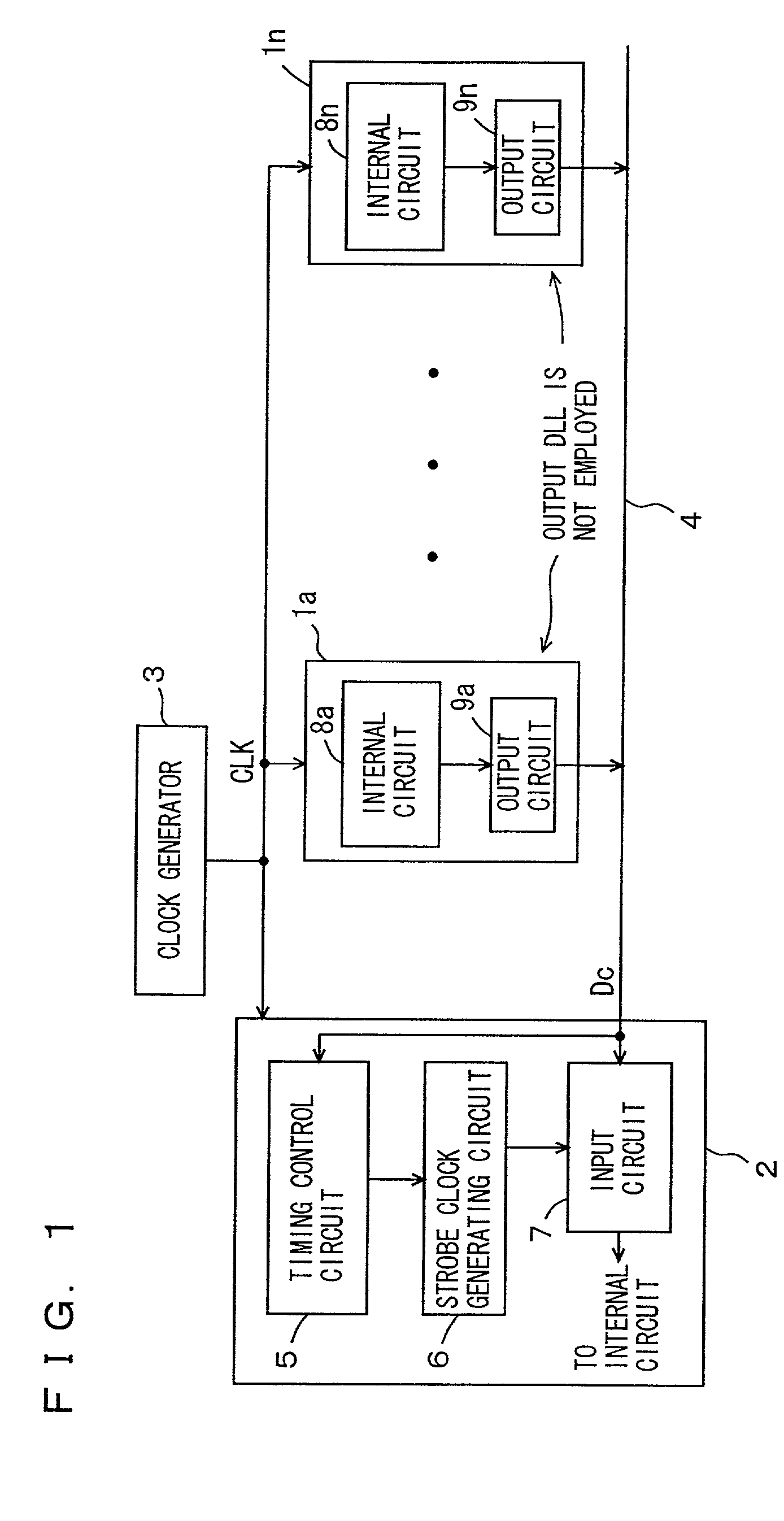
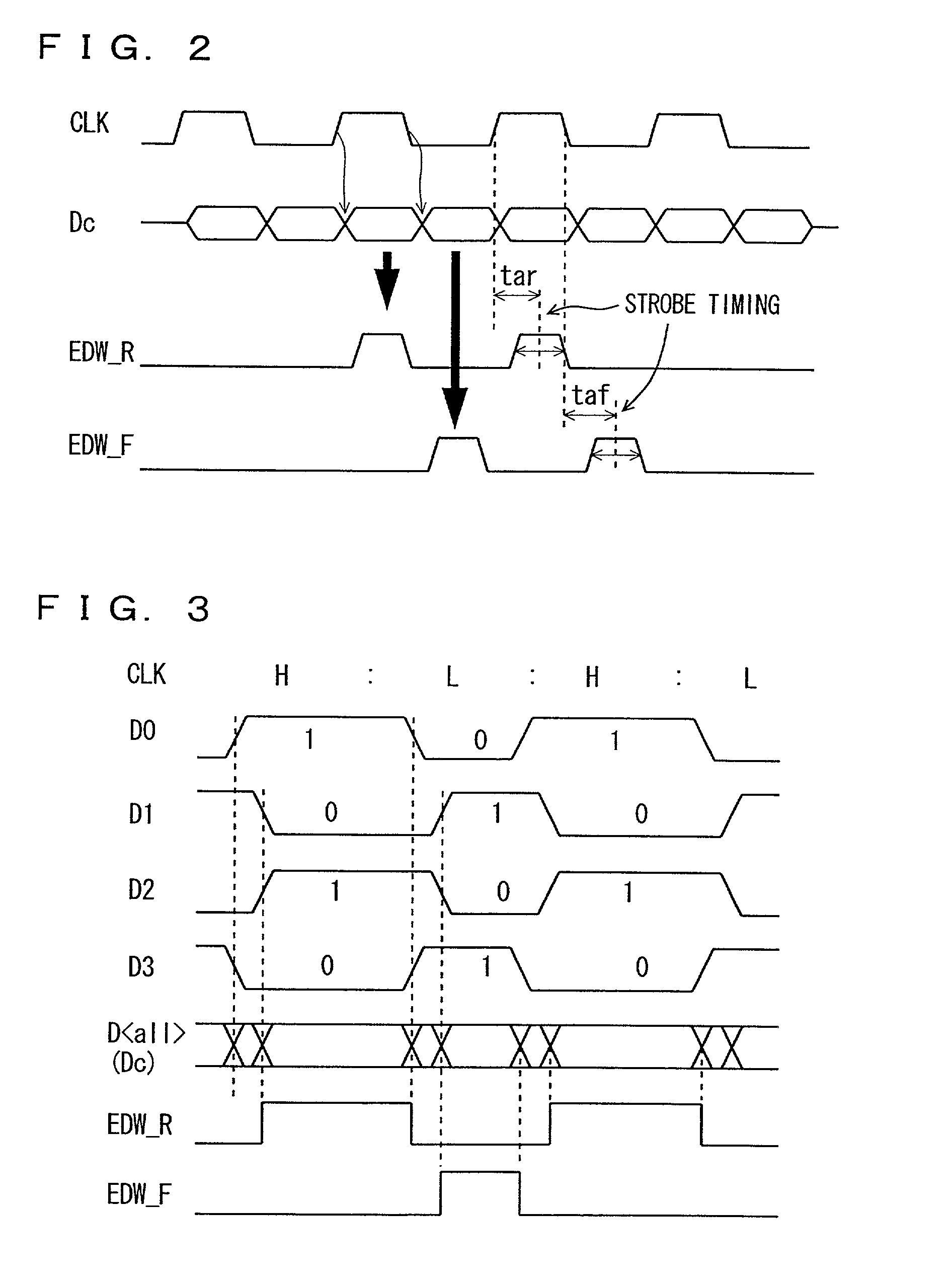
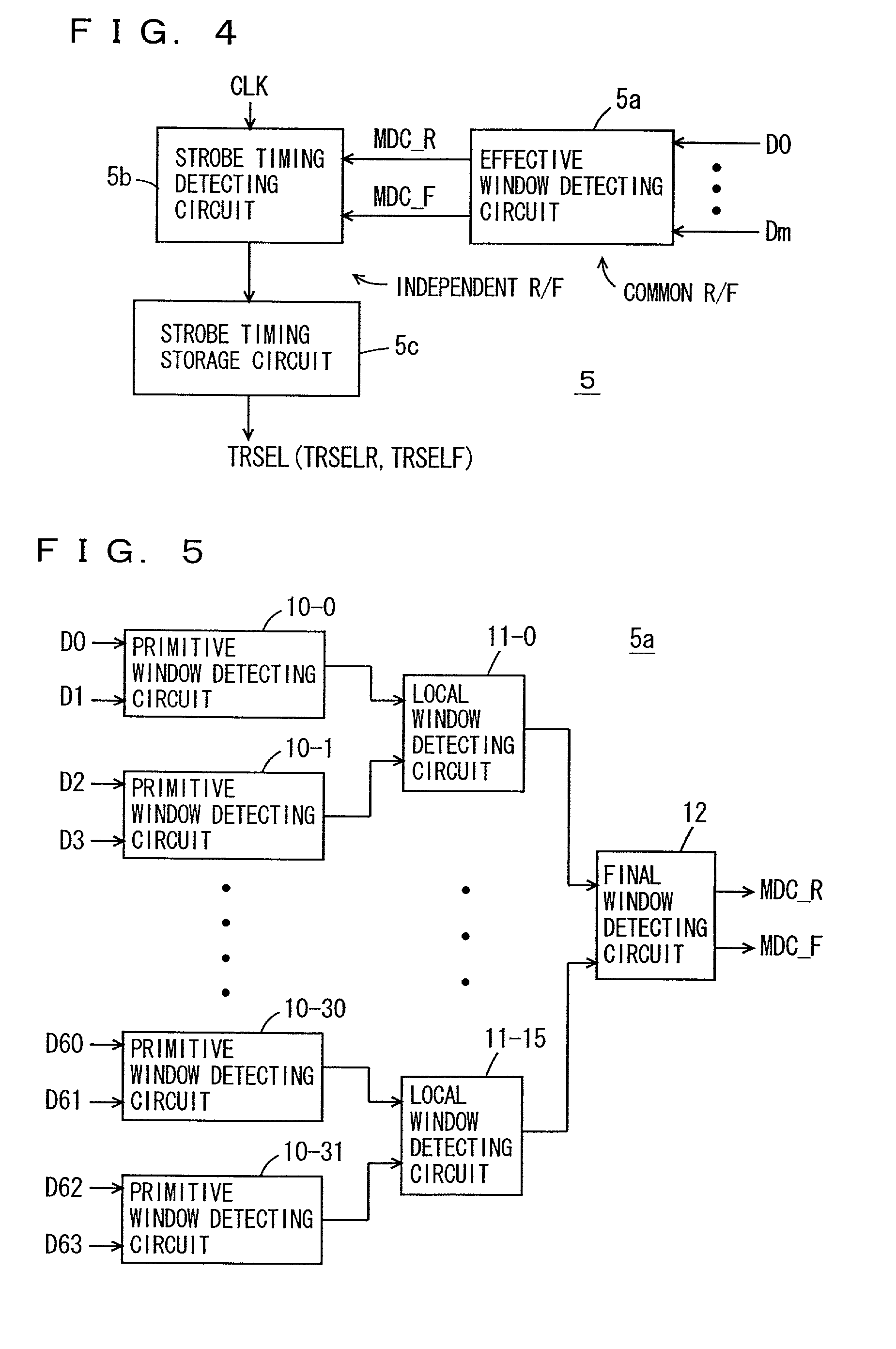
An interface unit includes a timing control circuit for extracting an effective data window by detecting a point of change in a transferred data, and determining strobe timing for taking in the data in accordance with the extracted effective window; and a strobe clock generating circuit for generating a strobe clock signal for taking in the data under control of the timing control circuit. Regardless of the system structure, accurate data transfer is achieved between any semiconductor devices in the system.

Description

[0001] 1. Field of the Invention[0002] The present invention relates to an interface circuit such as a memory control device for controlling access to a memory device, and in particular to a bus interface circuit for rapidly taking in data in synchronization with a clock signal.[0003] 2. Description of the Background Art[0004] FIG. 78 shows an example of a structure of a conventional data processing system. In FIG. 78, the conventional processing system includes a clock generator CG generating a system clock signal CLK, memory units MU0-MUn connected in parallel to a common bus CB and operating in synchronization with system clock signal CLK, a processor PC, such as a CPU (Central Processing Unit), for processing data stored in memory units MU0-MUn, and a memory controller MCR for transferring data requested of accessing by processor PC between memory units MU0-MUn and processor PC. Memory controller MCR operates in synchronization with system clock signal CLK as well.[0005] In such...

Claims


Application Information

Patent Timeline
Patent Type & Authority Applications(United States)
IPC IPC(8): G06F12/00G06F13/16G06F13/42G11C11/401G11C11/407
CPCG06F13/1689G06F13/4239Y02B60/1228Y02B60/1235Y02D10/00G06F12/00
Inventor KUGE, SHIGEHIRO
Owner RENESAS ELECTRONICS CORP
Learn More