PCB and method for making PCB with thin copper layer

Inactive Publication Date: 2001-07-19
TELEFON AB LM ERICSSON (PUBL)
View PDF0 Cites 0 Cited by
  • Summary
  • Abstract
  • Description
  • Claims
  • Application Information

AI Technical Summary

Benefits of technology

[0003] By means of the present invention, a circuit board has been produced, in which the material makes it possible for the linear expansion due to temperature increases to be reduced considerably, but in which it is still possible to have relatively thin copper layers and thus a fine-meshed pattern with conductor widths as small as 50 .mu.m. The board is still inexpensive in comparison with, for example, the variants with the metal cores. To this end, the invention is characterized in that the carrier layer has, at least in certain portions, been allowed to have a surface roughness of up to essentially the same size as the thickness of the copper layer, and in that, at least in the abovementioned portions, a surface-levelling plane layer is arranged between the carrier layer and the copper layer. The plane layer suitably consists of epoxy and has a thickness which is essentially the same size as the surface roughness of the carrier layer, that is to say is essentially the same thickness as the surface roughness of the carrier layer. In this connection, a carrier layer which contains glass fibre and epoxy can advantageously be used, and good linear expansion properties are achieved if the glass fibre content exceeds 70%.
[0006] In the case of those laminates which are to have through-plated holes, it is an advantage if these holes are drilled after application of epoxy but before the copper-plating because it is then possible to obtain a homogeneous copper thickness.

Problems solved by technology

One problem, especially with an advanced degree of miniaturization, is thermal expansion which can result in breakage and contact difficulties.
Another problem is surface roughness.
If the quantity of glass is increased, the thermal expansion coefficient decreases, but a disadvantage of this is that the surface of the laminate becomes coarser.
A secondary consequence of the surface becoming coarser, that is to say being imparted an inferior surface finish, is that, when copper plating is applied, it is not possible to have too thin a copper layer because the conductor pattern is jeopardized by the coarse surface.
On the other hand, with a thicker copper layer, it must be borne in mind that etching has to continue until those portions which are to be removed are completely etched through and removed, which means that the pattern cannot be made too fine-meshed because the etching becomes more uneven at the edges as the etching time increases and the risk of defects then increases.
There are circuit boards which have a low thermal expansion coefficient but these are in most cases based on cores of metal or ceramics and are relatively expensive.

Method used


Image

  • PCB and method for making PCB with thin copper layer

Examples


Embodiment Construction

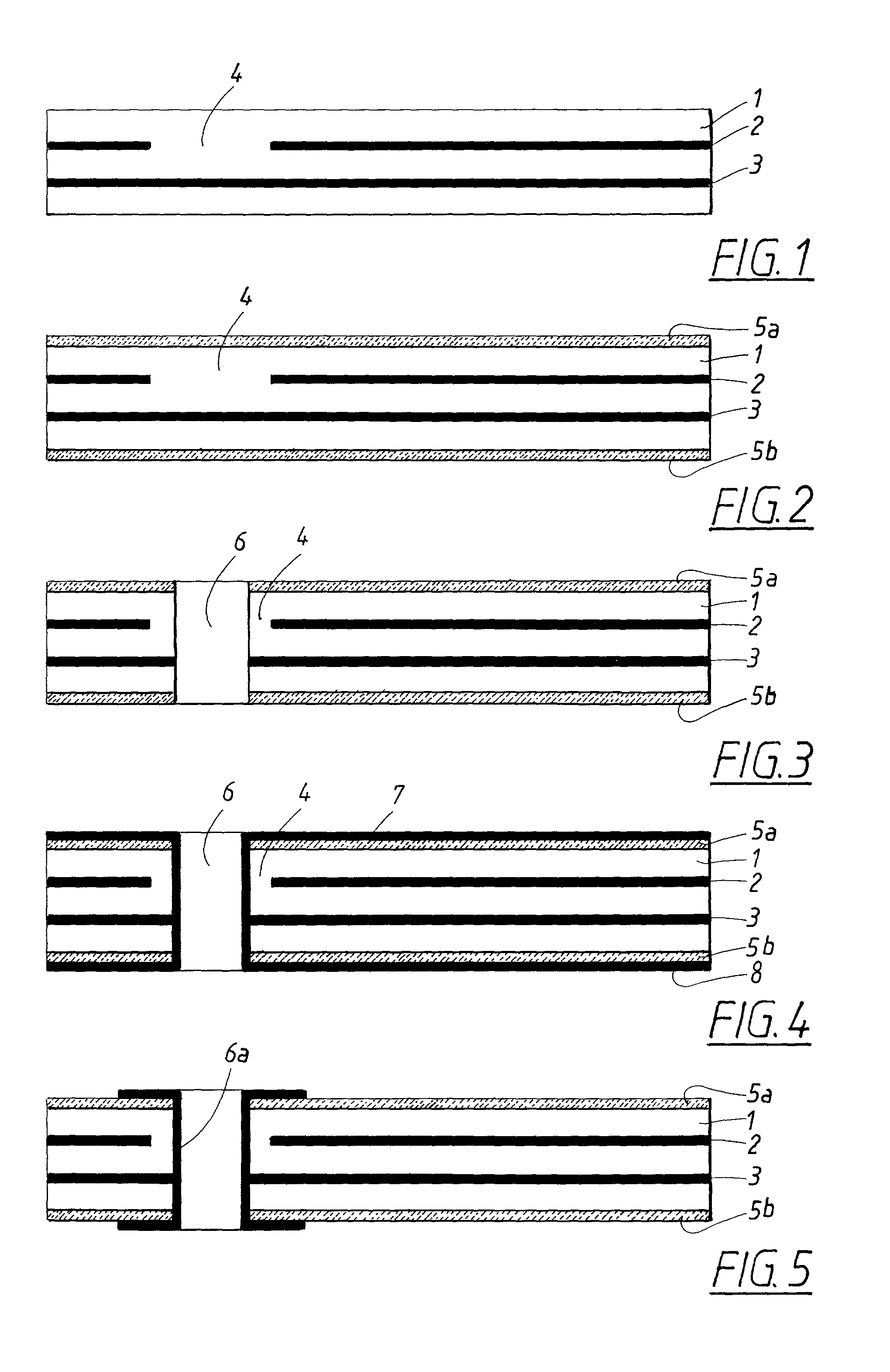
[0013] With reference to FIG. 1, the invention includes a laminate 1 made of glass fibre-filled epoxy. Included in the glass fibre laminate are two inner conductor layers 2 and 3. The conductor layer 2 is provided with an insulating hole 4 for subsequent drilling through without contact. The percentage of glass fibre / epoxy in the glass fibre layer is suitably 75 / 25, but glass contents as low as 70% are possible. With this high glass fibre content, a linear expansion coefficient as low as 9-10 ppm / .degree. C. is achieved, which is to be compared with the more usual 16-18 ppm for conventionally used circuit board laminates with glass fibre contents of 40-60%. A low linear expansion coefficient is desirable when the copper layer is thin, down towards 18-20 .mu.m, which is in turn the case when it is necessary to etch narrow conductors on account of an advanced degree of miniaturization. It is well known that etching narrow conductors requires a thin copper layer. However, with the abov...


PUM

PropertyMeasurementUnit
Fractionaaaaaaaaaa
Thicknessaaaaaaaaaa
Timeaaaaaaaaaa

Abstract

The invention concerns a PC board with laminates for electrical circuits, the PC board comprising at least one carrier (1) and at least one copper surface layer (7), intended to, after the removal of selected parts, e.g. by etching, function as conductors on the PC board. The new thing is that the carrier at least at some parts has a surface roughness of up to mainly the same size as the thickness of the copper layer and that at least at the above named rough parts is arranged a surface levelling layer (5a,b) between the carrier (1) and the copper layer (7). Further, the invention concerns a method for producing PC board laminate for electrical circuits as above, the laminate comprising a copper layer and a carrier that has a surface roughness of mainly the same size as the thickness of the copper layer. The new thing here is that a layer (5a,b) of liquid epoxy is applied on the one or those surface parts of the carrier which in the end are to carry a copper layer, that the epoxy layer is dried and hardened, and that copper layers (7) are plated on the epoxy layers (5a,b).

Description

[0001] The present invention relates to a printed circuit board made of laminate for electric circuits, comprising at least one carrier layer and at least one surface layer made of copper intended, after the removal of selected portions, for example by etching, to constitute the conductors on the board. The invention also relates to a method for producing printed circuit board laminate of the abovementioned type intended for electric circuits.[0002] Circuit boards with conductors consisting of a copper layer etched into a pattern located on one or both sides of the board or even inside the board are commonly used within the field of electronics. These boards often have a base layer consisting of glass fibre mixed with epoxy. The glass content in these mixtures can vary, but common values are 40-60%. One problem, especially with an advanced degree of miniaturization, is thermal expansion which can result in breakage and contact difficulties. Another problem is surface roughness. If t...

Claims


Application Information

Patent Timeline
IPC IPC(8): H05K1/03H05K3/38H05K3/42
CPCH05K1/0366H05K3/381H05K3/387H05K3/426H05K2203/0759Y10S428/901Y10T428/24917Y10T428/24355Y10T428/24994
Inventor BERGSTEDT, LEIFLIGANDER, PER
Owner TELEFON AB LM ERICSSON (PUBL)
Why Eureka
Try Eureka