Method of manufacturing a semiconductor element front side electrode
a semiconductor element and front side electrode technology, applied in the field of semiconductor elements, can solve the problems of higher production cost, increased nickel film thickness, and higher method production cos
- Summary
- Abstract
- Description
- Claims
- Application Information
AI Technical Summary
Benefits of technology
Problems solved by technology
Method used
Image

Examples
first embodiment
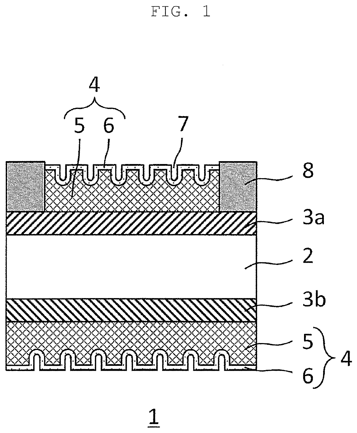
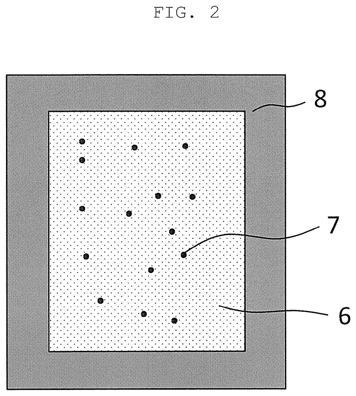
[0024]FIG. 1 is a schematic sectional view of a semiconductor element of a first embodiment. FIG. 2 is a schematic plan view of the semiconductor element of this embodiment.
[0025]In FIG. 1 and FIG. 2, a semiconductor element 1 of this embodiment includes: a front-back conduction-type substrate 2; a front-side electrode 3a formed on one main surface (front surface) of the front-back conduction-type substrate 2; a back-side electrode 3b formed on the other main surface (back surface) of the front-back conduction-type substrate 2; and electroless plating layers 4 formed on the front-side electrode 3a and the back-side electrode 3b. The electroless plating layers 4 include: electroless nickel-phosphorus plating layers 5 formed on the front-side electrode 3a and the back-side electrode 3b; and electroless gold plating layers 6 formed on the electroless nickel-phosphorus plating layers 5, and have formed on surfaces thereof a plurality of recesses 7. In addition, a protective film 8 is ar...
second embodiment
[0076]In a second embodiment, a suitable method of manufacturing the semiconductor element 1 of the first embodiment is described.
[0077]The manufacturing method of this embodiment includes the same basic steps as the manufacturing method of the first embodiment, and hence only differences therefrom are described.
[0078]In electroless gold plating treatment, nickel in an electroless nickel-phosphorus plating layer 5 is dissolved in an electroless gold plating solution, and an electroless gold plating layer 6 is formed by displacement between nickel and gold. At this time, as the nickel concentration of the electroless nickel-phosphorus plating layer 5 becomes larger, the amount of nickel dissolved in the electroless nickel-phosphorus plating layer 5 becomes larger. Moreover, as the amount of nickel dissolved in the electroless nickel-phosphorus plating layer 5 becomes larger, the recesses 7 are more easily formed on the surface of the electroless nickel-phosphorus plating layer 5.
[007...
third embodiment
[0088]In a third embodiment, a suitable method of manufacturing the semiconductor element 1 of the first embodiment is described.
[0089]The manufacturing method of this embodiment includes the same basic steps as the manufacturing method of the first embodiment, and hence only differences therefrom are described.
[0090]During electroless nickel-phosphorus plating treatment, a hydrogen gas is generated, and hence hydrogen gas bubbles adhere to the surface of an electroless nickel-phosphorus plating layer 5 having been deposited. The hydrogen gas bubbles microscopically reduce the deposition efficiency of the electroless nickel-phosphorus plating layer 5. Therefore, the thickness of the electroless nickel-phosphorus plating layer 5 is liable to become smaller in portions to which the hydrogen gas bubbles adhere than in portions to which the hydrogen gas bubbles do not adhere.
[0091]In view of the foregoing, in the method of manufacturing the semiconductor element 1 of this embodiment, th...
PUM
| Property | Measurement | Unit |
|---|---|---|
| thicknesses | aaaaa | aaaaa |
| thickness | aaaaa | aaaaa |
| thickness | aaaaa | aaaaa |
Abstract
Description
Claims
Application Information
 - R&D
- Intellectual Property
- Life Sciences
- Materials
- Tech Scout
- Unparalleled Data Quality
- Higher Quality Content
- 60% Fewer Hallucinations
Browse by: Latest US Patents, China's latest patents, Technical Efficacy Thesaurus, Application Domain, Technology Topic, Popular Technical Reports.
© 2025 PatSnap. All rights reserved.Legal|Privacy policy|Modern Slavery Act Transparency Statement|Sitemap|About US| Contact US: help@patsnap.com