Optical device and method for manufacturing optical device
a technology of optical devices and optical components, applied in the field of optical devices, can solve the problems that the configuration described above cannot be applied to a small and thin semiconductor package including a redistribution layer, and achieve the effect of light receiving efficiency
- Summary
- Abstract
- Description
- Claims
- Application Information
AI Technical Summary
Benefits of technology
Problems solved by technology
Method used
Image
Examples
first embodiment
Variations of First Embodiment
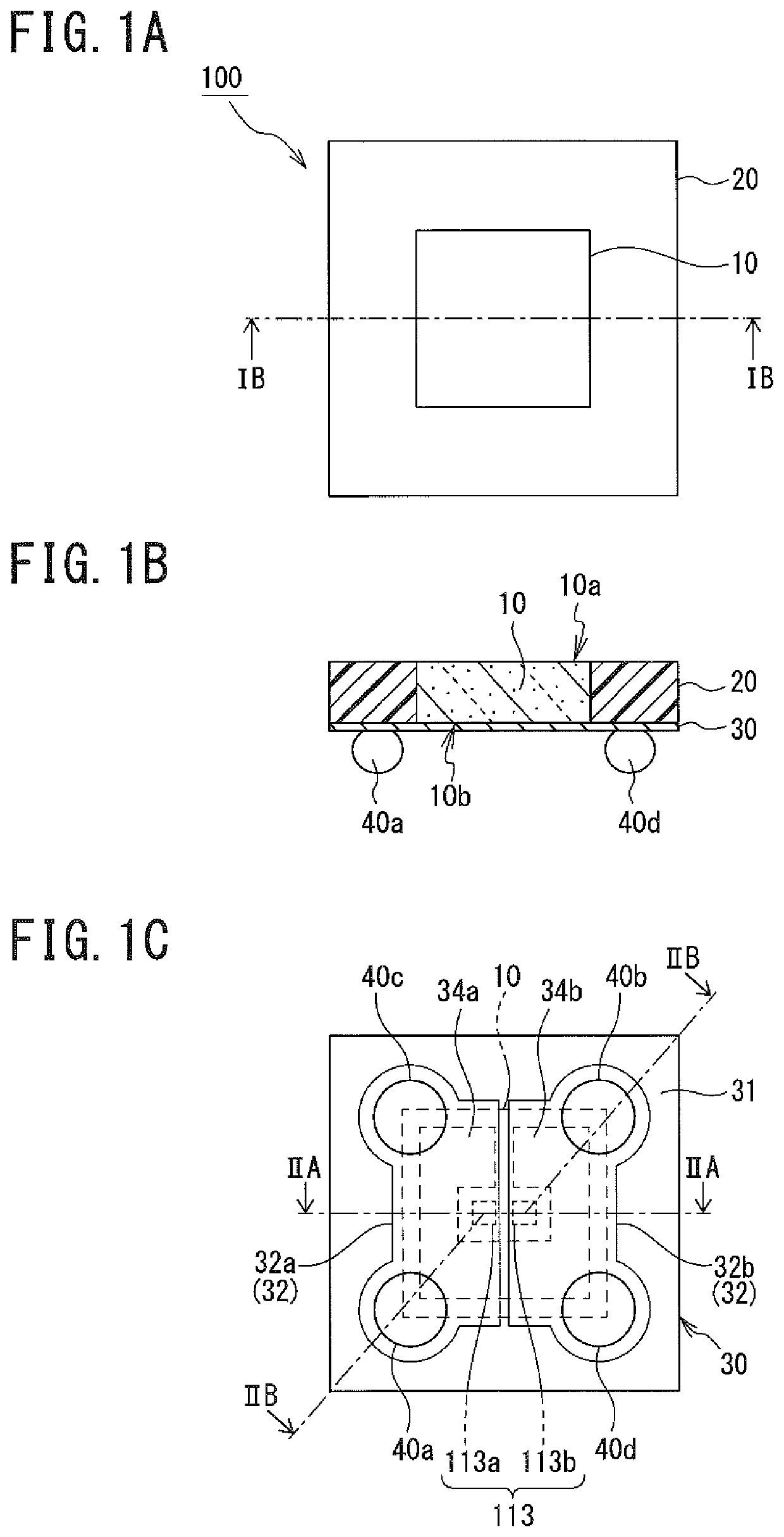
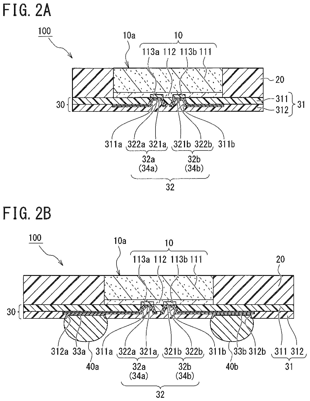
[0072](1) Although, regarding the optical device 100 according to the first embodiment, an example in which the light incident surface 10a of the photoelectric conversion element 10 is disposed at the same height (in an identical plane) as the upper surface of the sealing portion 20 was described, the present invention is not limited to such a configuration.
[0073]For example, the light incident surface 10a (when an antireflection coating is disposed, the upper surface of the antireflection coating) of the photoelectric conversion element 10 may be disposed at a position recessed from the upper surface of the sealing portion 20 (the surface of the sealing portion 20 on the opposite side to the redistribution layer 30). In this case, the sealing portion 20 functions as a view angle restriction portion that restricts an incidence angle of light incident on the photoelectric conversion element 10. While the photoelectric conversion elements 10 are separated...
second embodiment
2. Second Embodiment
[0082]Hereinafter, a second embodiment of the present invention will be described with reference to the drawings.
Configuration of Optical Device
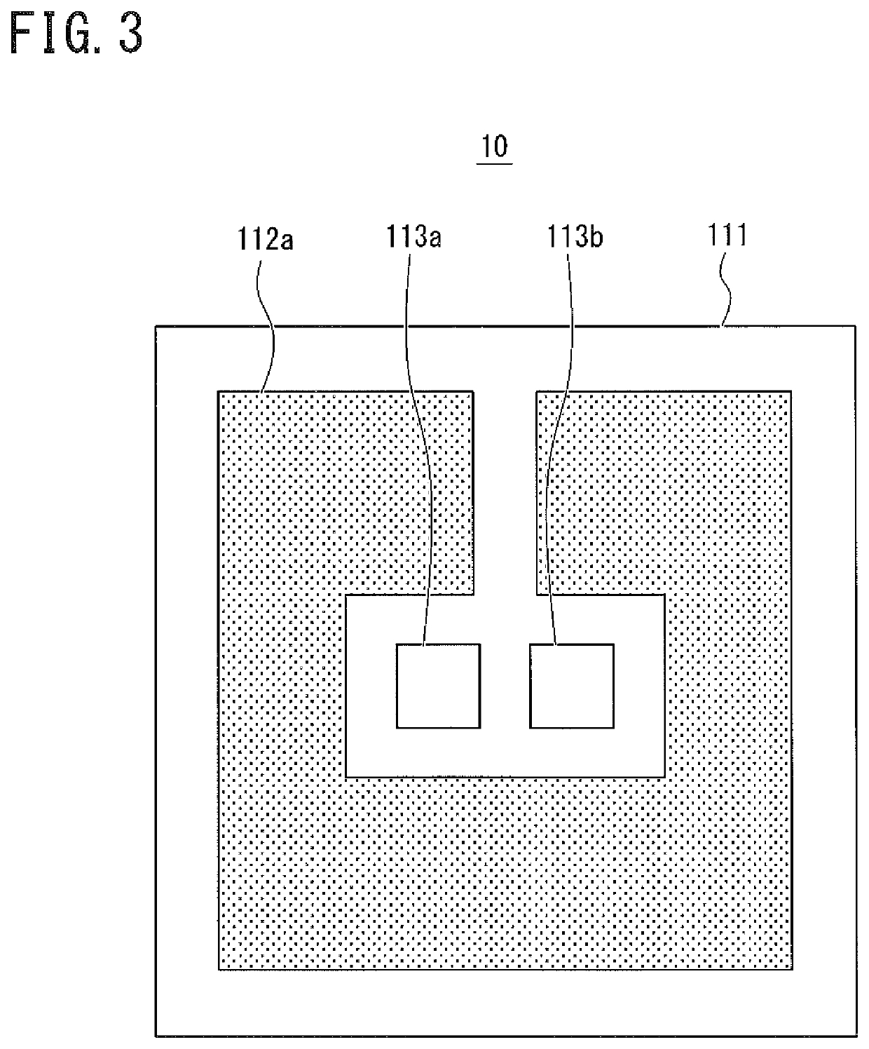
[0083]Using FIGS. 7A and 7B with reference to FIG. 3, a configuration of an optical device 200 according to the second embodiment will be described. FIGS. 7A and 7B are a bottom view of the optical device 200 and a cross-sectional view illustrative of a configuration in a cross-section taken along the line VIIB-VIIB of FIG. 7A, respectively. FIG. 7B is a cross-sectional view illustrated in such a manner that the bottom surface of the optical device 200 faces downward.
[0084]As illustrated in FIGS. 7A and 7B, the optical device 200 differs from the optical device 100 of the first embodiment in that the optical device 200 includes, in place of the redistributions 32 of the first embodiment, redistributions 232 having shapes different from those of the redistributions 32. The redistributions 232 include a first redistribution...
third embodiment
3. Third Embodiment
[0091]Hereinafter, a third embodiment of the present invention will be described with reference to the drawings.
Configuration of Optical Device
[0092]Using FIGS. 8A and 8B with reference to FIG. 3, a configuration of an optical device 300 according to the third embodiment will be described. FIGS. 8A and 8B are a bottom view of the optical device 300 and a cross-sectional view illustrative of a configuration in a cross-section taken along the line VIIIB-VIIIB of FIG. 8A, respectively. FIG. 8B is a cross-sectional view illustrated in such a manner that the bottom surface of the optical device 300 faces downward.
[0093]As illustrated in FIGS. 8A and 8B, the optical device 300 differs from the optical device 100 of the first embodiment in that the optical device 300 includes, in place of the redistributions 32 of the first embodiment, redistributions 332 having shapes different from those of the redistributions 32. The redistributions 332 include a first redistribution ...
PUM
| Property | Measurement | Unit |
|---|---|---|
| emissivity | aaaaa | aaaaa |
| width | aaaaa | aaaaa |
| area | aaaaa | aaaaa |
Abstract
Description
Claims
Application Information
 - R&D
- Intellectual Property
- Life Sciences
- Materials
- Tech Scout
- Unparalleled Data Quality
- Higher Quality Content
- 60% Fewer Hallucinations
Browse by: Latest US Patents, China's latest patents, Technical Efficacy Thesaurus, Application Domain, Technology Topic, Popular Technical Reports.
© 2025 PatSnap. All rights reserved.Legal|Privacy policy|Modern Slavery Act Transparency Statement|Sitemap|About US| Contact US: help@patsnap.com


