
Display cover substrate and display device including same

a technology of display cover and substrate, which is applied in the direction of photomechanical equipment, instruments, synthetic resin layered products, etc., can solve the problems of exposed organic electroluminescent display panels to ultraviolet light (uv), and achieve the effects of improving strength and reliability, and improving the hardness of the display cover substra

Active Publication Date: 2022-01-04
LG INNOTEK CO LTD
View PDF16 Cites 0 Cited by
  • Summary
  • Abstract
  • Description
  • Claims
  • Application Information

AI Technical Summary

Benefits of technology

[0011]A display cover substrate according to an embodiment can have improved strength and reliability.
[0012]Specifically, in the display cover substrate according to the embodiment, it is possible to have improved strength by disposing a surface reinforcing layer disposed on at least one of one surface and the other surface of a flexible substrate to improve the hardness of the display cover substrate.
[0013]In addition, the display cover substrate according to the embodiment can reduce a light transmittance in a specific wavelength region of light incident from the outside by disposing multiple functional layers on the surface reinforcing layer.
[0014]Specifically, the display cover substrate according to the embodiment can reduce a transmittance of UV light in a light wavelength band of about 388 nm or less.
[0015]Accordingly, when the display cover substrate according to the embodiment is applied to a display device, it is possible to reduce the incidence of UV light into a display panel disposed under the display cover substrate.
[0016]Thus, it is possible to prevent a self-luminous element disposed inside the display panel from being damaged or deformed by the ultraviolet rays, thereby improving the reliability and lifetime of the display device.

Problems solved by technology

Although it is possible to use an organic electroluminescent display panel to reduce the thickness of such a flexible display device, such an organic electroluminescent display panel is vulnerable to ultraviolet light (UV) introduced from the outside.

Method used


Image

  • Display cover substrate and display device including same
  • Display cover substrate and display device including same
  • Display cover substrate and display device including same

Examples


exemplary embodiment 1

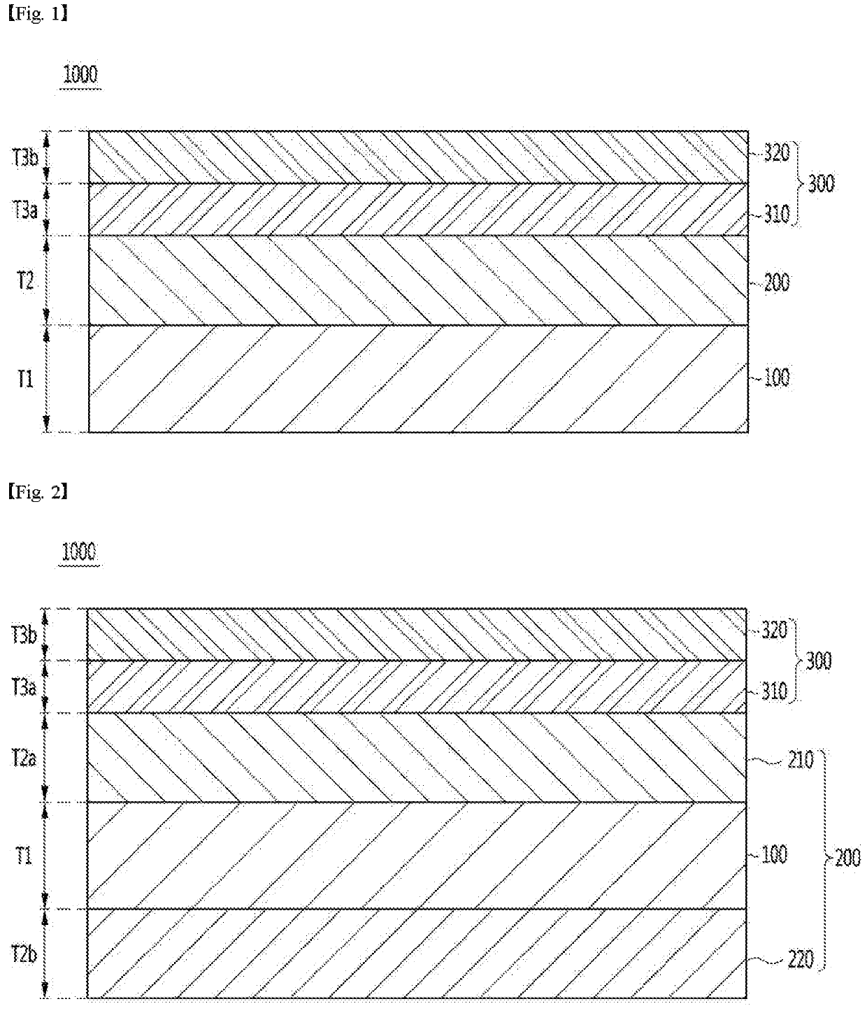
[0167]A surface reinforcing layer containing an acrylic resin was coated on a substrate containing polyimide.

[0168]Subsequently, a first layer containing titanium dioxide was disposed on the surface reinforcing layer, and a second layer containing silicon dioxide was disposed on the first layer to manufacture a display cover substrate.

[0169]At this time, a thickness of the first layer was 1 nm to 25 nm, and a thickness of the second layer was 80 nm to 120 nm.

[0170]Then, hardness of the display cover substrate and a light transmittance by a wavelength band were measured.

exemplary embodiment 2

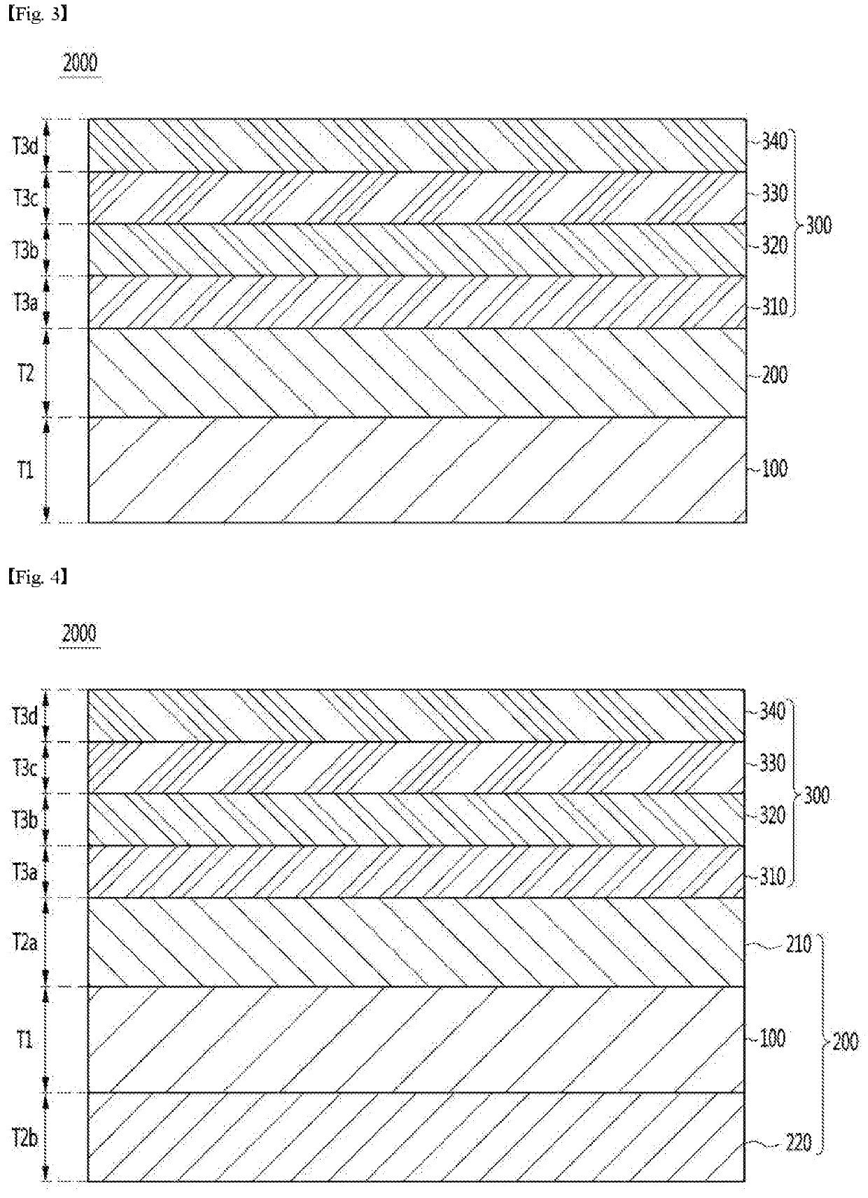
[0187]A surface reinforcing layer containing an acrylic resin was coated on a substrate containing polyimide.

[0188]Subsequently, a first layer containing titanium dioxide was disposed on the surface reinforcing layer, a second layer containing silicon dioxide was disposed on the first layer, a third layer containing zirconium dioxide was disposed on the second layer, and a fourth layer containing silicon dioxide was disposed on the third layer to manufacture a display cover substrate.

[0189]At this time, a thickness of the first layer was 10 nm to 25 nm, a thickness of the second layer was 10 nm to 50 nm, a thickness of the third layer was 110 nm to 200 nm, and a thickness of the fourth layer was 25 nm to 110 nm.

[0190]Then, hardness of the display cover substrate and a light transmittance by a wavelength band were measured.

exemplary embodiment 3

[0205]A surface reinforcing layer containing an acrylic resin was coated on a substrate containing polyimide.

[0206]Subsequently, a first layer containing zirconium dioxide was disposed on the surface reinforcing layer, a second layer containing silicon dioxide was disposed on the first layer, a third layer containing zirconium dioxide was disposed on the second layer, and a fourth layer containing silicon dioxide was disposed on the third layer to manufacture a display cover substrate.

[0207]At this time, a thickness of the first layer was 10 nm to 50 nm, a thickness of the second layer was 10 nm to 50 nm, a thickness of the third layer was 40 nm to 70 nm, and a thickness of the fourth layer was 60 nm to 120 nm.

[0208]Then, hardness of the display cover substrate and a light transmittance by a wavelength band were measured.


PUM

PropertyMeasurementUnit
light transmittanceaaaaaaaaaa

Abstract

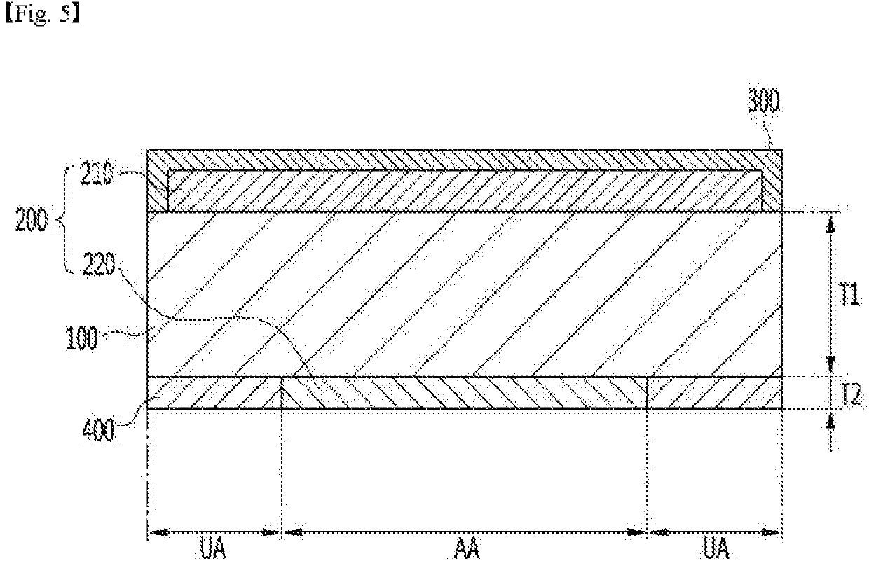
A display cover substrate according to an embodiment includes: a flexible substrate including one surface and the other surface opposite to the one surface; a surface reinforcing layer disposed on the one surface; and a functional layer disposed on the surface reinforcing layer, wherein the functional layer includes a plurality of layers having different refractive indexes, and an average light transmittance is 90% or more in a light wavelength band of 388 nm to 700 nm, and an average light transmittance is less than 90% and a minimum light transmittance is 60% or less in a light wavelength band of 250 nm to 388 nm.

Description

CROSS REFERENCE TO RELATED APPLICATIONS[0001]This application is the National Phase of PCT International Application No. PCT / KR2017 / 014666, filed on Dec. 13, 2017, which claims priority under 35 U.S.C. 119(a) to Patent Application No. 10-2016-0172302, filed in the Republic of Korea on Dec. 16, 2016 and Patent Application No. 10-2017-0017425, filed in the Republic of Korea on Feb. 8, 2017, all of which are hereby expressly incorporated by reference into the present application.TECHNICAL FIELD[0002]Embodiments relate to a display cover substrate and a display device including the same.BACKGROUND ART[0003]Recently, a bendable display device has been applied to various electronic appliances. For example, there is an increasing interest in display devices that are bent in at least one direction and foldable.[0004]For example, when such a flexible display device is folded in half, it can be used in a smartphone, and when a screen is unfolded, it can be applied to an IT device which can be...

Claims


Application Information

Patent Timeline
Patent Type & Authority Patents(United States)
IPC IPC(8): H01L51/52G06F3/044
CPCH01L51/524G06F3/0443H01L2251/303H01L2251/5338H01L2251/558B32B7/02B32B27/06B32B27/28B32B27/36G03F7/028H10K50/841H10K2102/311H10K2102/00H10K2102/351
Inventor KIM, JONG SUNPARK, DUCK HOONPARK, JAE SEOKSHIN, JUN SIKCHOE, YU LIMHAN, YU MI
Owner LG INNOTEK CO LTD
Learn More