
Semiconductor device and method for manufacturing semiconductor device

a semiconductor device and semiconductor technology, applied in semiconductor devices, diodes, electrical devices, etc., can solve the problems of reducing the resistance of voltage, further ionizing collision, and destroying the semiconductor device, so as to prevent excessive erosion, high activity, and high activity loss

Active Publication Date: 2020-09-22
MITSUBISHI ELECTRIC CORP
View PDF14 Cites 1 Cited by
  • Summary
  • Abstract
  • Description
  • Claims
  • Application Information

AI Technical Summary

Benefits of technology

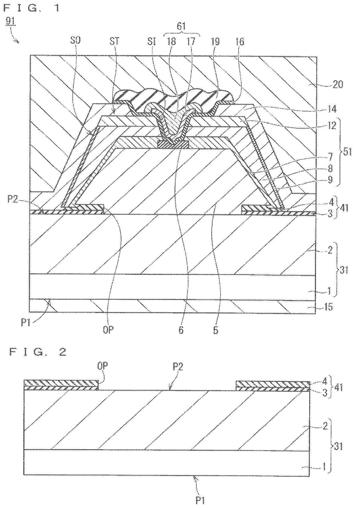
[0021]According to the one aspect of the present invention, the second p-type epitaxial layer is not an implanted layer formed through ion implantation, but an epitaxial layer. The second p-type epitaxial layer thus has high activity while being a p-type gallium-nitride-based material. Further, the second p-type epitaxial layer is disposed on the outer side wall, which forms the smaller angle than the right angle together with the second surface of the semiconductor substrate. That is, the second p-type epitaxial layer constitutes the outer side wall of the stack made of the gallium-nitride-based material, the outer side wall being inclined at a gentler angle than a right angle with respect to the semiconductor substrate. Hence, there is no need to etch the second p-type epitaxial layer for exposure as a preparation for joining the source electrode portion to the second p-type epitaxial layer. This prevents excessive erosion of the second p-type epitaxial layer and the loss of the high activity of the second p-type epitaxial layer due to the etching. As described above, the second p-type epitaxial layer, being in contact with the source electrode portion, has high activity. This achieves favorable ohmic contact between them. Accordingly, holes generated by an ionizing collision during the operation of the semiconductor device are efficiently retrieved to the source electrode portion. This improves the avalanche strength of the semiconductor device.
[0022]According to the other aspect of the present invention, the p-type epitaxial layer is disposed not only on the top surface of the stack, but also on the side wall of the stack. Accordingly, a pn junction is established not only in the vicinity of the top surface, but also in the vicinity of the side wall. A depletion layer extending from the pn junction in the vicinity of the side wall to all over the n-type epitaxial layer lessens an electric field at a Schottky interface between the n-type barrier layer and the anode electrode. This enhances the reverse withstand voltage of the semiconductor device. Further, the p-type epitaxial layer is not a p-type layer formed through ion implantation, but an epitaxial layer. The second p-type epitaxial layer thus has high activity while being a p-type gallium-nitride-based material. This further sufficiently achieves the aforementioned effect.

Problems solved by technology

This likely causes a reduction in withstand voltage.
This causes a further ionizing collision.
Such a phenomenon destroys the semiconductor device in the end.

Method used


Image

  • Semiconductor device and method for manufacturing semiconductor device
  • Semiconductor device and method for manufacturing semiconductor device
  • Semiconductor device and method for manufacturing semiconductor device

Examples


first embodiment

Summary of Configuration

[0063]FIG. 1 is a schematic cross-sectional view of a configuration of a semiconductor device (MOSFET) 91 in a first embodiment. The following items (1) to (5) summarize the configuration of the semiconductor device 91.

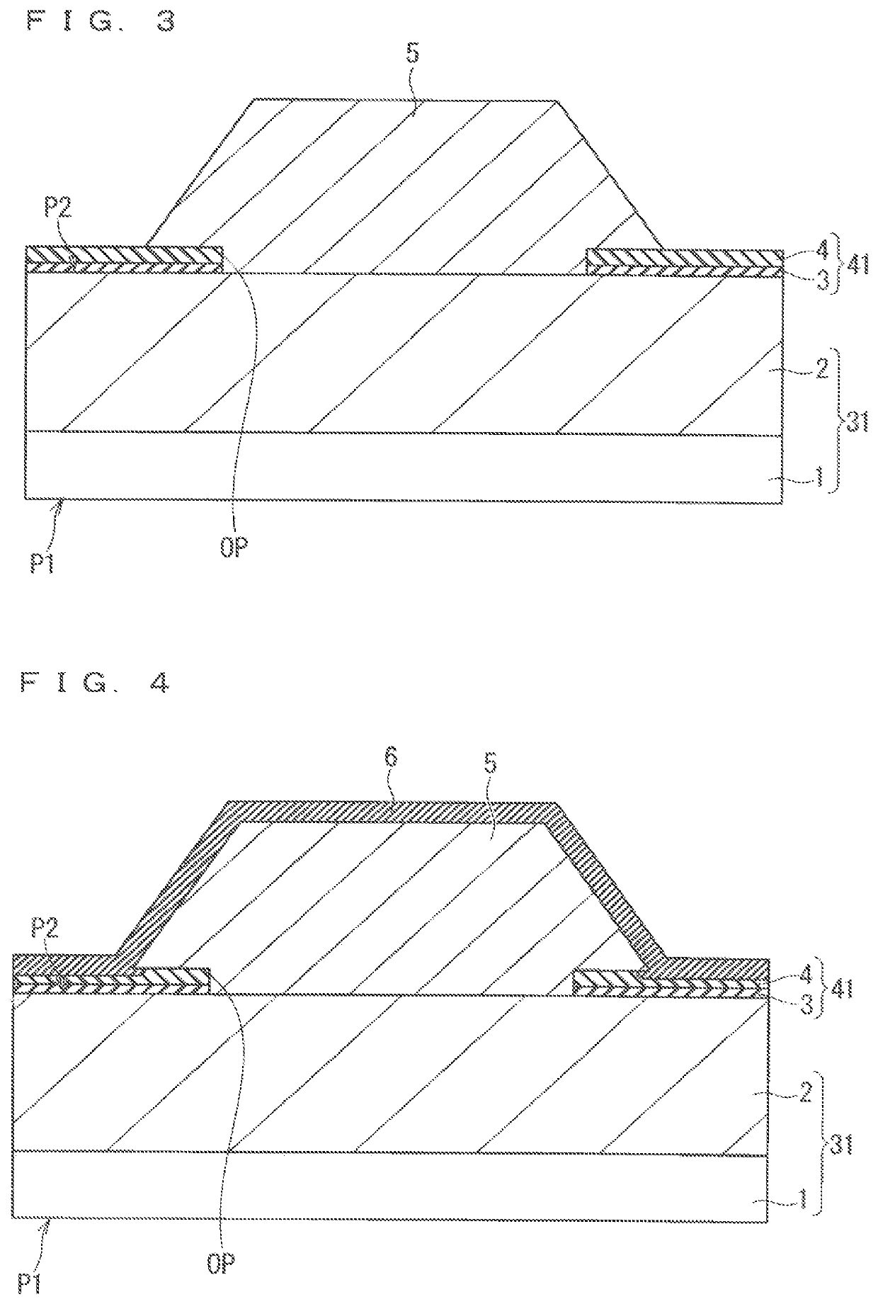
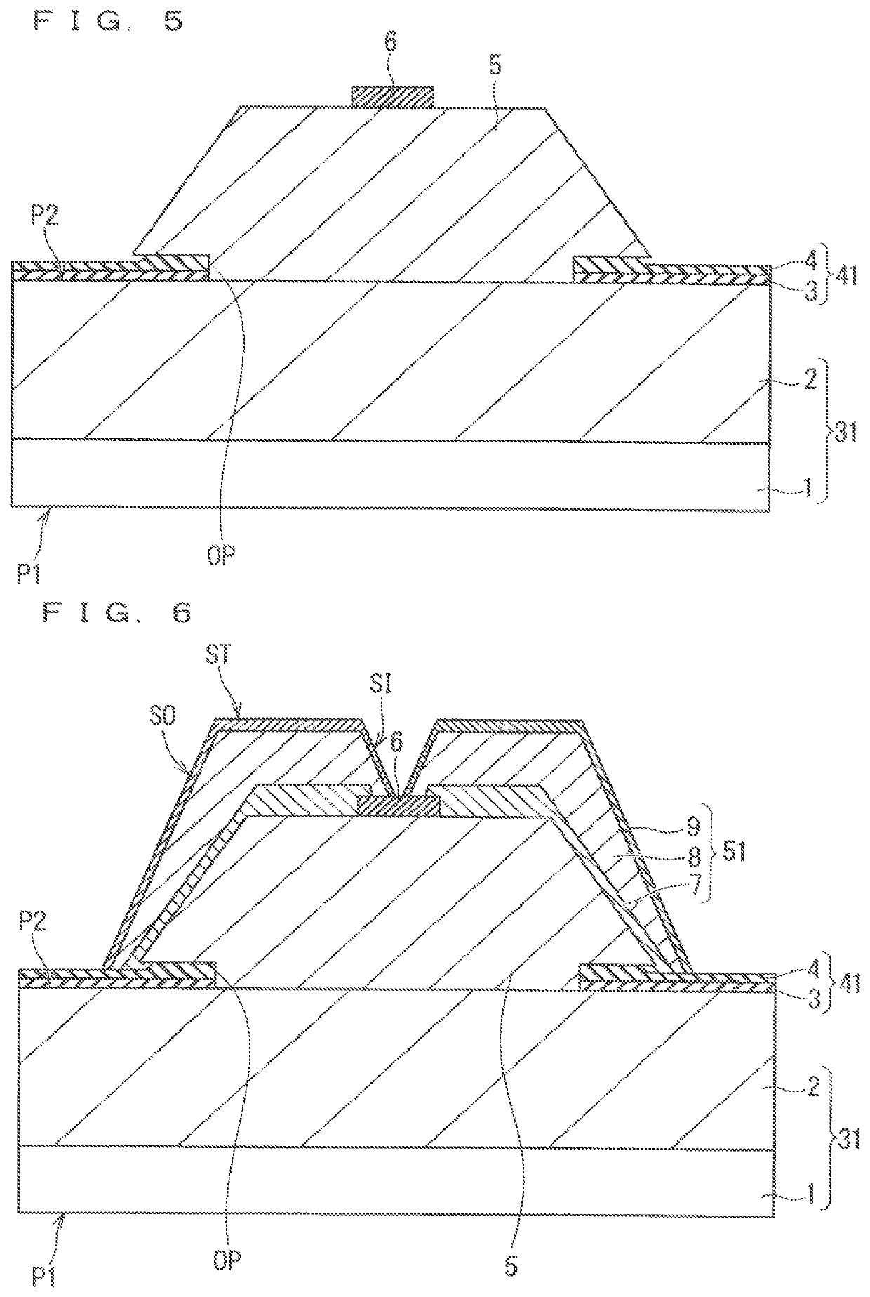
[0064](1) The semiconductor device 91 includes a semiconductor substrate (epitaxial substrate) 31, a first insulating layer 41, a second insulating layer 6, a stack 51, an n-type contact layer 12, a source electrode portion 14, a drain electrode 15, a gate insulating film 16, and a gale electrode 61. The semiconductor substrate 31 has a first surface (lower surface) P1 and a second surface P2 (upper surface) opposite the first surface P1. The first insulating layer 41 is disposed on the second surface P2 of the semiconductor substrate 31, and has an opening OP partly exposing the second surface P2. The second insulating layer 6 is disposed on the second surface P2 of the semiconductor substrate 31, and separated from the first insulating layer ...

second embodiment

[0145]FIG. 27 is a schematic cross-sectional view of a configuration of a MOSFET (semiconductor device) 92 in a second embodiment. The MOSFET 91 (FIG. 1: the first embodiment) is configured such that an epitaxial growth layer tends to have a large total thickness. This tendency is advantageous to obtain high withstand voltage, but involves high resistance of the drift layer, thereby easily increasing the on-resistance. Accordingly, when a low on-resistance is a high priority, provided is a possible configuration in which the bottom n-type epitaxial layer 5 of the MOSFET 91 is omitted, like the MOSFET 92, to reduce the resistance of the drift layer. This reduces the on-resistance.

[0146]In a method for manufacturing the MOSFET 92, a process of forming the bottom n-type epitaxial layer 5 (FIG. 3) is omitted. This simplifies a process. Further, as a result of this omission, a step of forming a second insulating layer 6V (FIG. 27) can be performed at the same time as the step of forming ...

third embodiment

Summary of Configuration

[0149]FIG. 28 is a schematic cross-sectional view of a configuration of a semiconductor device (diode) 93 in a third embodiment. The following item (1) summarizes the configuration of the semiconductor device 93.

[0150](1) The semiconductor device 93 includes a semiconductor substrate (epitaxial substrate) 31, an insulating layer 42, a stack 53, an n-type barrier Layer 12D, an anode electrode 25, and a cathode electrode 24. The semiconductor substrate 31 has a first surface (lower surface) P1 and a second surface P2 (upper surface) opposite the first surface P1. The insulating layer 42 is disposed on the second surface P2 of the semiconductor substrate 31, and has an opening OP partly exposing the second surface P2. The stack 53 includes an n-type epitaxial layer 7D and a p-type epitaxial layer 9D in sequence on the second surface P2 of the semiconductor substrate 31. The n-type epitaxial layer 7D and the p-type epitaxial layer 9D are made of a gallium-nitride...


PUM

PropertyMeasurementUnit
thicknessaaaaaaaaaa
thicknessaaaaaaaaaa
thicknessaaaaaaaaaa

Abstract

A first insulating layer is disposed on a second surface of a semiconductor substrate, and has an opening. A second insulating layer is disposed on the second surface and separated from the first insulating layer. A stack includes, in sequence on the second surface, a side n-type epitaxial layer and first and second p-type epitaxial layers that are made of a gallium-nitride-based material. The stack has an outer side wall having a portion formed of the second p-type epitaxial layer, an inner side wall extending from the second insulating layer, and a top surface. The n-type contact layer is disposed on the top surface. The source electrode portion is in contact with the n-type contact layer on the top surface, and is in contact with the second p-type epitaxial layer on the outer side wall. A gate insulating film is disposed on the inner side wall.

Description

TECHNICAL FIELD[0001]The present invention relates to semiconductor devices and methods for manufacturing the semiconductor devices, and more particularly, to a semiconductor device made of a gallium-nitride-based material and a method for manufacturing the semiconductor device.BACKGROUND ART[0002]Semiconductor devices including wide bandgap semiconductors have been actively developed in recent years. One of the wide bandgap semiconductors particularly with hope is a gallium-nitride (GaN)-based material. Hence, techniques relating to the GaN-based material such as a technique of epitaxial layer formation and a microprocessing technique of processing an epitaxial layer into a desired shape have been studied.[0003]Non-Patent Document 1 studies a selective growth technique of growing an epitaxial layer into a desired shape with application to optical semiconductor devices, such as a laser and an ultraviolet detector in view. The GaN-based material is promisingly available to power semi...

Claims


Application Information

Patent Timeline
Patent Type & Authority Patents(United States)
IPC IPC(8): H01L29/06H01L29/12H01L29/868H01L29/861H01L29/872H01L29/40H01L29/20H01L29/423H01L29/417H01L21/306H01L21/28H01L29/51H01L21/02H01L21/265H01L29/66H01L29/78H01L29/08H01L29/36H01L29/10
CPCH01L29/0847H01L29/42376H01L29/517H01L29/66522H01L29/868H01L29/513H01L29/42364H01L21/28264H01L21/0254H01L29/0692H01L29/872H01L29/06H01L21/02636H01L29/36H01L29/861H01L29/41758H01L29/4236H01L29/66212H01L21/26546H01L29/78H01L29/12H01L29/0649H01L21/30625H01L29/2003H01L29/1095H01L29/7789H01L29/7813H01L29/7802H01L29/0657H01L29/66734H01L29/045
Inventor HAYASHIDA, TETSURONANJO, TAKUMA
Owner MITSUBISHI ELECTRIC CORP
Learn More