Method of controlling ion energy distribution using a pulse generator with a current-return output stage

Active Publication Date: 2019-10-15
APPLIED MATERIALS INC
View PDF167 Cites 14 Cited by
  • Summary
  • Abstract
  • Description
  • Claims
  • Application Information

AI Technical Summary

Benefits of technology

This patent describes a method for processing a substrate using a plasma generated over the surface of the substrate. The method includes using a pulsed voltage waveform to create a single peak ion energy distribution function (IEDF) that can be used to create an IEDF with an arbitrary shape. The method includes using a current-return output stage to minimize voltage spikes that may occur during the rapid release of magnetic energy. The technical effect of the patent is the ability to maintain a nearly constant sheath voltage for up to about 90% of the substrate processing time, resulting in a more precise plasma operation and improved substrate processing.

Problems solved by technology

Reliably producing high aspect ratio features is one of the key technology challenges for the next generation of very large scale integration (VLSI) and ultra large scale integration (ULSI) of semiconductor devices.
When a lower frequency, e.g., 2 MHz, RF bias generator is used to get higher self-bias voltages, the difference in energy between these two peaks can be significant; and because the etch profile due to the ions at low energy peak is more isotropic, this could potentially lead to bowing of the feature walls.
The authors have further noticed that this cannot be accomplished by simply applying a DC voltage to a power electrode.
As a result, the unbalanced net current from the bulk plasma (equal to the ion current) is constantly charging the substrate surface, which ultimately leads to all of the applied DC voltage being dropped across the substrate and a dielectric layer of the ESC assembly (i.e., chuck capacitor) instead of across the plasma sheath (i.e., sheath capacitor) as desired.

Method used


Image

  • Method of controlling ion energy distribution using a pulse generator with a current-return output stage
  • Method of controlling ion energy distribution using a pulse generator with a current-return output stage
  • Method of controlling ion energy distribution using a pulse generator with a current-return output stage

Examples


Embodiment Construction

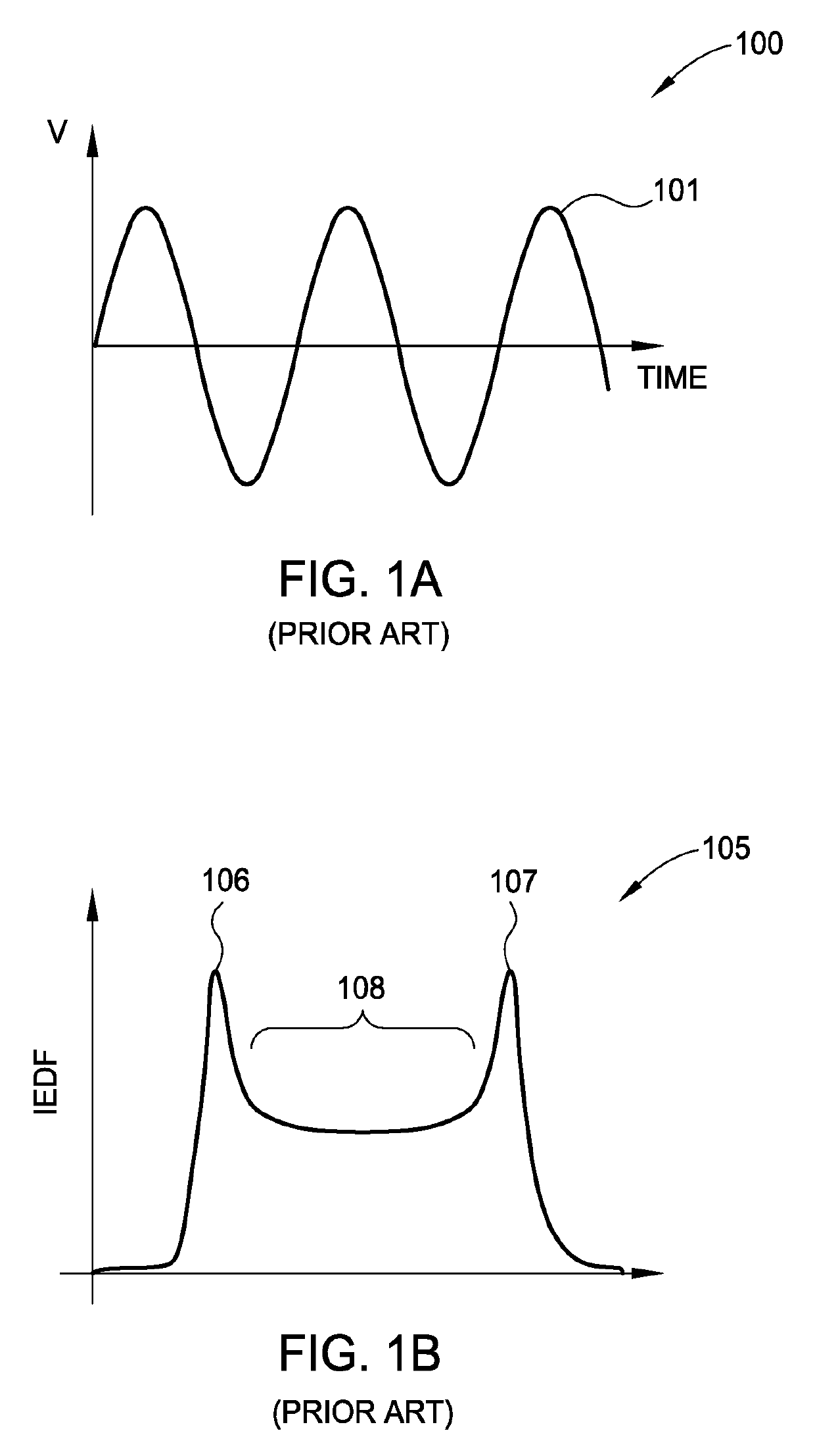
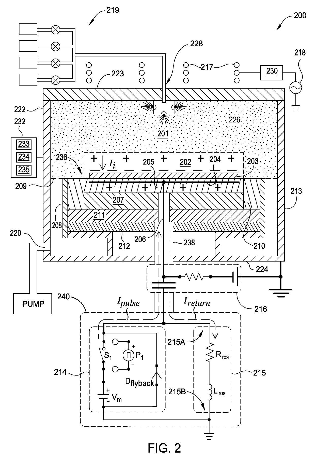
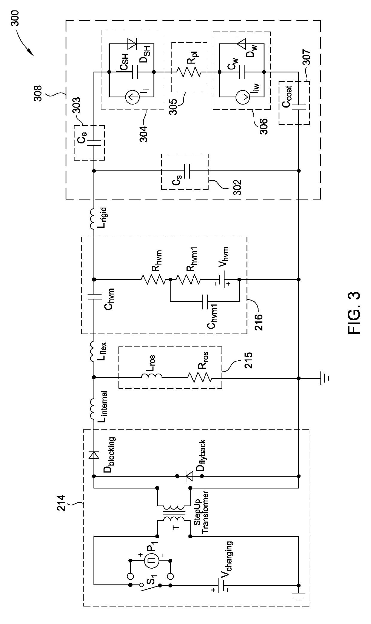
[0025]Embodiments described herein are applicable to all plasma assisted or plasma enhanced processing chambers and methods of plasma assisted or plasma enhanced processing of a substrate. More specifically, embodiments of this disclosure describe an electrode biasing scheme that enables maintaining a nearly constant sheath voltage and thus creating a mono-energetic IEDF at the surface of the substrate; consequently enabling a precise control over the shape of IEDF and the profile of the features formed in the surface of the substrate. The following definitions are used throughout this disclosure: (1) unless a reference is specified, all potentials are referenced to ground; (2) the voltage at any physical point (like a substrate or a biasing electrode) is likewise defined as the potential of this point with respect to ground (zero potential point); (3) the cathode sheath is implied to be an electron-repelling, ion-accelerating sheath that corresponds to a negative substrate potentia...


PUM

PropertyMeasurementUnit
Timeaaaaaaaaaa
Timeaaaaaaaaaa
Fractionaaaaaaaaaa

Abstract

Embodiments of this disclosure describe an electrode biasing scheme that enables maintaining a nearly constant sheath voltage and thus creating a mono-energetic IEDF at the surface of the substrate that consequently enables a precise control over the shape of IEDF and the profile of the features formed in the surface of the substrate.

Description

CROSS-REFERENCE TO RELATED APPLICATIONSField[0001]This application is a continuation of U.S. patent application Ser. No. 15 / 976,728, filed on May 10, 2018, which is herein incorporated by reference in its entirety.BACKGROUNDField[0002]Embodiments described herein generally relate to plasma processing chambers used in semiconductor manufacturing.Description of the Related Art[0003]Reliably producing high aspect ratio features is one of the key technology challenges for the next generation of very large scale integration (VLSI) and ultra large scale integration (ULSI) of semiconductor devices. One method of forming high aspect ratio features uses a plasma assisted etching process, such as a reactive ion etch (RIE) plasma process, to form high aspect ratio openings in a material layer, such as a dielectric layer, of a substrate. In a typical RIE plasma process, a plasma is formed in an RIE processing chamber and ions from the plasma are accelerated towards a surface of a substrate to f...

Claims


Application Information

Patent Timeline
IPC IPC(8): H01J37/32H05H1/46H01J37/34H01J37/08C23C14/34C23C14/54
CPCH01J37/32146H01J37/32577H01L21/67069H01J2237/3341H01J2237/3348H01J37/32174H01J37/3426H01J37/3438H01J37/3444H01J37/3467H05H1/46C23C16/505H01L21/3065H01L21/31116H01L21/32136H01J37/248H01J37/08C23C14/345C23C14/3485C23C14/54H05H2242/20
Inventor DORF, LEONIDLUERE, OLIVIERDHINDSA, RAJINDERROGERS, JAMESSRINIVASAN, SUNILMISHRA, ANURAG KUMAR
Owner APPLIED MATERIALS INC
Why Eureka
Try Eureka