Current sensing circuit with a current-compensated drain voltage regulation

Active Publication Date: 2006-08-29
INFINEON TECH LLC
View PDF11 Cites 21 Cited by
  • Summary
  • Abstract
  • Description
  • Claims
  • Application Information

AI Technical Summary

Benefits of technology

[0011]One or more aspects of the present invention serve to maintain a relatively constant voltage at a drain of a memory cell by compensating for parasitic behavior that may occur within a bitline decoding path. A relatively constant voltage can similarly be maintained at a protection node adjacent to the memory cell by compensating for parasitic behavior in a preamplifier path. The voltage at the protection node is generally maintained at the same level as the drain voltage. This mitigates the development of side leakage currents between the memory cell and the adjacent protection node. Compensating for parasitics and maintaining substantially constant voltages at these nodes mitigates margin loss and facilitates more reliable data sensing.
[0012]According to one or more aspects of the present invention, a circuit is disclosed that is configured to maintain a substantially constant voltage at a drain of a memory cell. The voltage is maintained by compensating for parasitics within a bitline decoding path. The circuit includes a current compensating feedback component that facilitates adjustments to the drain voltage Vd by adjusting a DATAB voltage on the bitline decoding path as a function of a current Icore flowing through the bitline decoding path, where the current flowing through the bitline decoding path results in a voltage drop across the bitline parasitics which reduces the drain voltage. Adjusting the DATAB voltage compensates for the voltage drop across the bitline parasitics to thereby maintain the drain voltage Vd at a substantially constant level.
[0013]According to one or more other aspects of the present invention, a circuit is disclosed that is configured to maintain a substantially constant voltage at a protection node adjacent to a drain of a memory cell to mitigate leakage currents from arising between the drain and the protection node. The voltage is maintained by compensating for parasitics within a preamplifier path. The circuit includes a current compensating feedback component that facilitates adjustments to the protection node voltage Vp by adjusting a PRE voltage on the preamplifier path as a function of a current Ip flowing through the preamplifier path, where the current flowing through the preamplifier path results in a voltage drop across the preamplifier parasitics which reduces the protection node voltage. Adjusting the PRE voltage compensates for the voltage drop across the preamplifier parasitics to thereby maintain the protection node voltage Vp at a substantially constant level.

Problems solved by technology

For example, DRAM and SRAM allow individual bits of data to be erased one at a time, but such memory loses its data when power is removed.
Alternatively, EEPROM can be easily erased without extra exterior equipment, but has reduced data storage density, lower speed, and higher cost.
This can, however, cause certain undesirable phenomena to become more prevalent.
For example, isolating two bits or charges stored within a charge trapping layer becomes increasingly difficult as the channel length is decreased and the individual bits are brought closer together within the charge trapping layer.
For example, the stored charges can contaminate or interfere with one another as they are brought closer together.
This can, for example, cause a current developed in a memory cell during a read operation to seem inordinately high, which can lead to a mistaken interpretation of a logic high or “1” when, in fact, the read should have yielded a logic low or “0”.
Such “mis-reads” can also be exacerbated by parasitic effects that can be experienced when reading a memory cell, as well as by current leakage that may occur in a “virtual ground” type architecture.

Method used


Image

  • Current sensing circuit with a current-compensated drain voltage regulation
  • Current sensing circuit with a current-compensated drain voltage regulation
  • Current sensing circuit with a current-compensated drain voltage regulation

Examples


Embodiment Construction

[0024]One or more aspects of the present invention are described with reference to the drawings, wherein like reference numerals are generally utilized to refer to like elements throughout, and wherein the various structures are not necessarily drawn to scale. In the following description, for purposes of explanation, numerous specific details are set forth in order to provide a thorough understanding of one or more aspects of the present invention. It may be evident, however, to one skilled in the art that one or more aspects of the present invention may be practiced with a lesser degree of these specific details. In other instances, well-known structures and devices are shown in block diagram or other form in order to facilitate describing one or more aspects of the present invention.

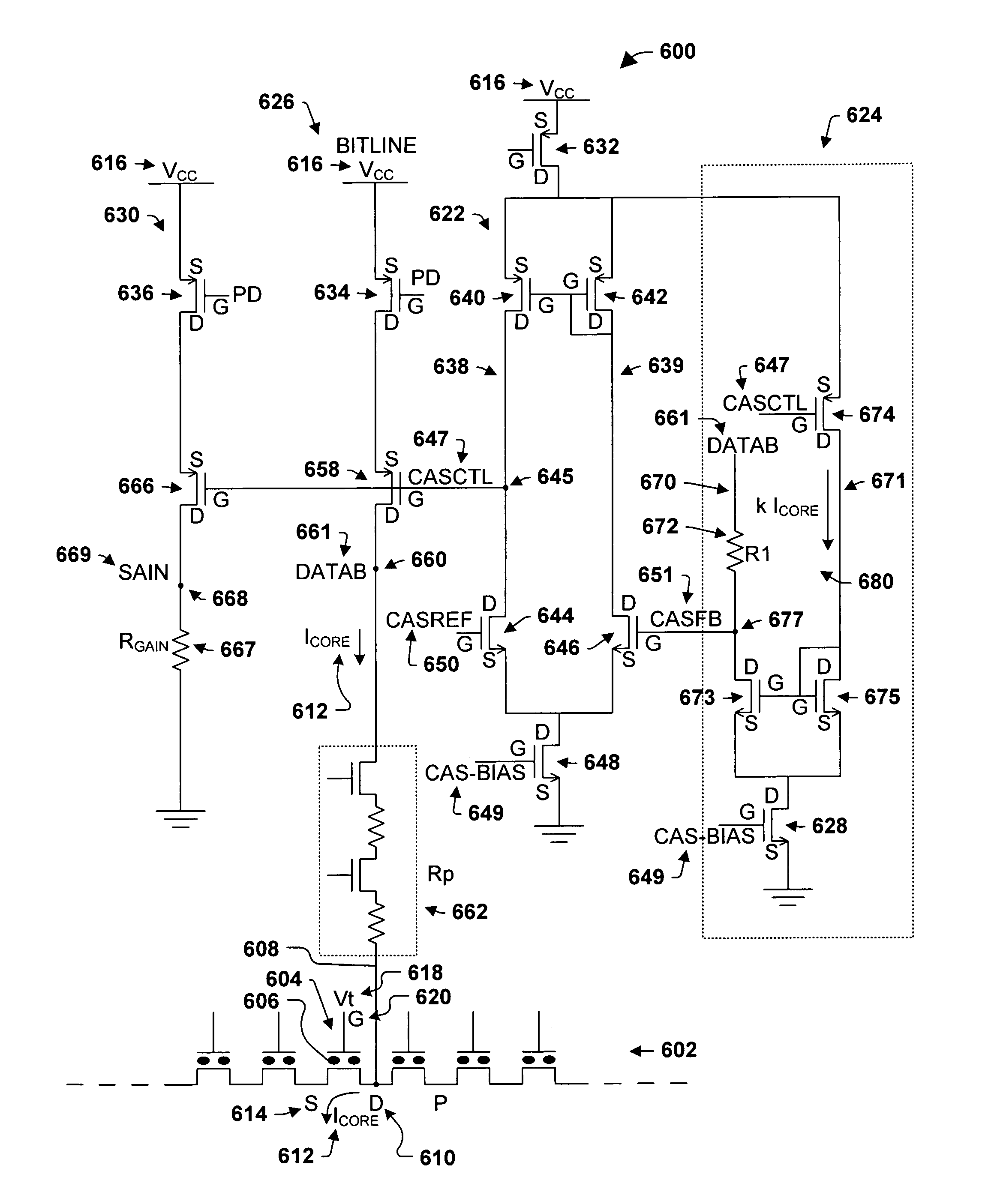
[0025]The present invention promotes more accurate data reads by maintaining a substantially constant voltage at one or more desired nodes. By way of example, prior art FIG. 1 represents a top view of...


PUM


Abstract

The present invention facilitates more accurate data reads by compensating for parasitic behavior—thus regulating the voltage at the drain of a core memory cell rather than at the output of a sensing circuit. More particularly, respective voltages at one or more nodes, such as the start of a bitline at a sensing circuit, for example, are adjusted to compensate for voltage drops that may occur due to parasitic behavior. Maintaining the substantially constant voltage levels at core memory cells allows comparisons to be made under ideal conditions while reducing the side leakages in virtual ground schemes. This mitigates margin loss and facilitates more reliable data sensing.

Description

FIELD OF INVENTION[0001]The present invention relates generally to memory for electronic systems and the like, and in particular to managing parasitic losses and leakage currents that may develop when reading a memory cell.BACKGROUND OF THE INVENTION[0002]Many different types memory exist to store data for computers and the like. For example, random access memory (RAM), dynamic random access memory (DRAM), static random access memory (SRAM), read only memory (ROM), programmable read only memory (PROM), electrically programmable read only memory (EPROM), electrically erasable programmable read only memory (EEPROM) and flash memory are all presently available to provide for data storage.[0003]Each type of memory has its own particular advantages and disadvantages. For example, DRAM and SRAM allow individual bits of data to be erased one at a time, but such memory loses its data when power is removed. Alternatively, EEPROM can be easily erased without extra exterior equipment, but has ...

Claims


Application Information

Patent Timeline
IPC IPC(8): G11C7/00
CPCG11C7/067G11C7/12G11C11/5642G11C16/24G11C16/28G11C16/30G11C29/026G11C16/0475G11C7/06G11C16/04G11C2207/063G11C2029/1204G11C5/147
Inventor WADHWA, SAMEERVENKATESH, BHIMACHAR
Owner INFINEON TECH LLC
Why Eureka
Try Eureka